Instructions:
- The marks are indicated in the right-hand margin.
- There are NINE questions in this paper.
- Attempt FIVE questions in all.
- Question No. 1 is compulsory.
Q.1 Choose the correct answer from the following (Any seven questions
only):
Which of these is used for amplification?
Which terminal in JFET controls the current?
BJT used as a switch operates in:
What is the built-in potential typically across a silicon p-n junction?
What is the peak inverse voltage for a center-tap full-wave rectifier?
Zener diode is mostly used in:
In MOSFET, the gate terminal is:
The voltage gain of a voltage follower (buffer amplifier) is:
In 2's complement method, what is the 2's complement of binary number 0101?
Which of the following is a universal gate?
Q.2 Solve both questions :
Explain the construction and working of an Enhancement Type MOSFET and draw its characteristics.
Define operating point. Explain the concept of load line analysis with suitable diagrams.
Q.3 Solve both questions :
With a neat diagram, explain the working of a Zener diode as a voltage regulator and draw its V-I characteristics.
Describe the three configurations of BJT (CE, CB, CC) and their applications.
Q.4 Solve both questions :
Derive the Shockley equation for JFET and explain the parameters involved.
Explain the difference between intrinsic and extrinsic semiconductors with suitable energy band diagrams.
Q.5 Solve both questions :
Discuss the role of filter circuits in rectifier applications. Explain the capacitor filter with waveforms.
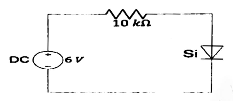
Determine the value of the current through the diode circuit given below. Assume $ V_\gamma = 0.7 \, V $.
Q.6 Solve both questions :
Convert $(0.513)_{10}$ to octal.
Explain how an Op-Amp integrator works and derive the output expression.
Q.7 Solve both questions :
Discuss the mechanism of breakdown in a diode. Differentiate between Zener and Avalanche breakdown.
Find the output of the Op-amp. Assume Op-amp is ideal.

Q.8 Solve both questions :
Explain the working of a Half Wave Rectifier and derive the expressions for average and RMS values of output voltage.
Implement an XOR gate using NAND gates.
Q.9 Write short notes on any two of the following:
Instructions:
- The marks are indicated in the right-hand margin.
- There are NINE questions in this paper.
- Attempt FIVE questions in all.
- Question No. 1 is compulsory.
Q.1 Choose the correct answer from the following (Any seven questions
only):
Which of these is used for amplification?
Which terminal in JFET controls the current?
BJT used as a switch operates in:
What is the built-in potential typically across a silicon p-n junction?
What is the peak inverse voltage for a center-tap full-wave rectifier?
Zener diode is mostly used in:
In MOSFET, the gate terminal is:
The voltage gain of a voltage follower (buffer amplifier) is:
In 2's complement method, what is the 2's complement of binary number 0101?
Which of the following is a universal gate?
Q.2 Solve both questions :
Explain the construction and working of an Enhancement Type MOSFET and draw its characteristics.
Define operating point. Explain the concept of load line analysis with suitable diagrams.
Q.3 Solve both questions :
With a neat diagram, explain the working of a Zener diode as a voltage regulator and draw its V-I characteristics.
Describe the three configurations of BJT (CE, CB, CC) and their applications.
Q.4 Solve both questions :
Derive the Shockley equation for JFET and explain the parameters involved.
Explain the difference between intrinsic and extrinsic semiconductors with suitable energy band diagrams.
Q.5 Solve both questions :
Discuss the role of filter circuits in rectifier applications. Explain the capacitor filter with waveforms.
Determine the value of the current through the diode circuit given below. Assume $ V_\gamma = 0.7 \, V $.

Q.6 Solve both questions :
Convert $(0.513)_{10}$ to octal.
Explain how an Op-Amp integrator works and derive the output expression.
Q.7 Solve both questions :
Discuss the mechanism of breakdown in a diode. Differentiate between Zener and Avalanche breakdown.
Find the output of the Op-amp. Assume Op-amp is ideal.
Q.8 Solve both questions :
Explain the working of a Half Wave Rectifier and derive the expressions for average and RMS values of output voltage.
Implement an XOR gate using NAND gates.
Q.9 Write short notes on any two of the following:
Instructions:
- The marks are indicated in the right-hand margin.
- There are NINE questions in this paper.
- Attempt FIVE questions in all.
- Question No. 1 is compulsory.
Q.1 Answer the following questions (any seven) :
Derive the relation between $ \beta $ and $ \alpha $ of a transistor. What is reverse leakage current in CE configuration?
What is modulation index in AM?
What is the concept of frequency reuse in cellular network?
What is the use of offset null input in the operational amplifier? How are they used?
Why is negative feedback desired in amplifier application?
Emitter bias or self-bias is more stable than fixed bias. Justify.
Explain how the process of avalanche breakdown occurs in a P-N junction diode. How is it different from Zener breakdown?
Justify that $ \overline{m}_j = M_j $ where $ m_j $ and $ M_j $ are th minterm (product term) and maxterm (sum term) respectively.
Mention the disadvantages of Wien bridge oscillator.
Mention the applications of one-shot multivibrator.
Q.2 Solve both questions :
Draw the waveform of output voltage $ V_0 $ if input is square wave and explain the operation of circuit given below.

Calculate the $ I_{RMS} $, $ I_{DC} $, ripple factor, rectification efficiency and PIV of rectifier circuit given below.

Q.3 Solve both questions :
For the network of figure given below, determine the following parameters using the approximate equivalent model: Voltage gain $ A_v $, Current gain $ A_i $, Input impedance $ Z_i' $ and $ Z_i $.

Draw the circuit diagram of voltage-series feedback amplifier and derive the expression of closed-loop voltage gain.
Q.4 Solve both questions :
Explain the operation performed by circuit given below and derive the expression of output voltage $ V_0 $.

Op-amp can be used to subtract the DC voltages (subtraction operation). Draw the circuit and explain the operation of subtractor using op-amp in non-inverting mode.
Q.5 Solve both questions :
Draw and explain the GSM signalling protocol architecture.
What is the need of modulation? Draw the wave shape of modulating signal, carrier signal and modulated wave in amplitude modulation.
Q.6 Solve both questions :
Draw the functional block diagram and explain the operation of monostable multi-vibrator using IC 555 timer.
Draw the basic circuit of an R-C phase-shift oscillator and explain its operation. If $ R_1 = R_2 = R_3 = 400 \text{ k}\Omega $ and $ C_1 = C_2 = C_3 = 50 \text{ pF} $, determine the frequency of oscillation in phase-shift oscillator.
Q.7 Solve both questions :
Implement the function $ F(A,B,C) = \Sigma(1,3,4,6,7) $ using $ 8 \times 1 $ MUX. Use A, B and C as selection line in which C is LSB and A is MSB.
Design 3-bit binary incrementer/decrementer circuit with the help of gates. When inputs are 000 and control pin is low, output should be 111. When inputs are 111 and control pin is high, output should be 000. For other combinations of inputs, when control pin is high, output should be incremented by one and when control pin is low, output should be decremented by one.
Q.8 Solve both questions :
Design a combinational circuit to check that two numbers $ A = (A_3A_2A_1A_0) $ and $ B = (B_3B_2B_1B_0) $ are equal with the help of gates. Output should be indicated by X. Output line X should be high if $ A = B $.
Design $ 8 \times 3 $ priority encoder with the help of basic gates.
Q.9 Solve both questions :
Compare the function and architecture of microprocessor and microcontroller.
Draw the input-output and transfer characteristics of CE amplifier.
Instructions:
- The marks are indicated in the right-hand margin.
- There are NINE questions in this paper.
- Attempt FIVE questions in all.
- Question No. 1 is compulsory.
Q.1 Answer the following questions (any seven) :
Derive the relation between $ \beta $ and $ \alpha $ of a transistor. What is reverse leakage current in CE configuration?
What is modulation index in AM?
What is the concept of frequency reuse in cellular network?
What is the use of offset null input in the operational amplifier? How are they used?
Why is negative feedback desired in amplifier application?
Emitter bias or self-bias is more stable than fixed bias. Justify.
Explain how the process of avalanche breakdown occurs in a P-N junction diode. How is it different from Zener breakdown?
Justify that $ \overline{m}_j = M_j $ where $ m_j $ and $ M_j $ are th minterm (product term) and maxterm (sum term) respectively.
Mention the disadvantages of Wien bridge oscillator.
Mention the applications of one-shot multivibrator.
Q.2 Solve both questions :
Draw the waveform of output voltage $ V_0 $ if input is square wave and explain the operation of circuit given below.
Calculate the $ I_{RMS} $, $ I_{DC} $, ripple factor, rectification efficiency and PIV of rectifier circuit given below.
Q.3 Solve both questions :
For the network of figure given below, determine the following parameters using the approximate equivalent model: Voltage gain $ A_v $, Current gain $ A_i $, Input impedance $ Z_i' $ and $ Z_i $.
Draw the circuit diagram of voltage-series feedback amplifier and derive the expression of closed-loop voltage gain.
Q.4 Solve both questions :
Explain the operation performed by circuit given below and derive the expression of output voltage $ V_0 $.
Op-amp can be used to subtract the DC voltages (subtraction operation). Draw the circuit and explain the operation of subtractor using op-amp in non-inverting mode.
Q.5 Solve both questions :
Draw and explain the GSM signalling protocol architecture.
What is the need of modulation? Draw the wave shape of modulating signal, carrier signal and modulated wave in amplitude modulation.
Q.6 Solve both questions :
Draw the functional block diagram and explain the operation of monostable multi-vibrator using IC 555 timer.
Draw the basic circuit of an R-C phase-shift oscillator and explain its operation. If $ R_1 = R_2 = R_3 = 400 \text{ k}\Omega $ and $ C_1 = C_2 = C_3 = 50 \text{ pF} $, determine the frequency of oscillation in phase-shift oscillator.
Q.7 Solve both questions :
Implement the function $ F(A,B,C) = \Sigma(1,3,4,6,7) $ using $ 8 \times 1 $ MUX. Use A, B and C as selection line in which C is LSB and A is MSB.
Design 3-bit binary incrementer/decrementer circuit with the help of gates. When inputs are 000 and control pin is low, output should be 111. When inputs are 111 and control pin is high, output should be 000. For other combinations of inputs, when control pin is high, output should be incremented by one and when control pin is low, output should be decremented by one.
Q.8 Solve both questions :
Design a combinational circuit to check that two numbers $ A = (A_3A_2A_1A_0) $ and $ B = (B_3B_2B_1B_0) $ are equal with the help of gates. Output should be indicated by X. Output line X should be high if $ A = B $.
Design $ 8 \times 3 $ priority encoder with the help of basic gates.
Q.9 Solve both questions :
Compare the function and architecture of microprocessor and microcontroller.
Draw the input-output and transfer characteristics of CE amplifier.
Instructions:
- The marks are indicated in the right-hand margin.
- There are NINE questions in this paper.
- Attempt FIVE questions in all.
- Question No. 1 is compulsory.
Q.1 Answer the following questions (any seven):
Why is negative feedback desired in amplifier application?
Draw the voltage transfer curve of op-amp.
State the Barkhausen's criteria for electronic system to oscillate with feedback.
How is amplifier different from the oscillator?
Why is the reception in the case of amplitude modulation usually noisy?
What is cell splitting and how does it increase the capacity of cellular network?
Justify that BJT is current controlled while FET is voltage-controlled device.
Name the breakdown mechanism in the lightly doped P-N junction diode under reverse biased condition.
Why is Gray code also called as reflected code? Convert $(396)_{10}$ to Gray code.
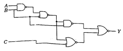
For the logical circuit shown in the figure, derive the simplified Boolean expression for output Y.
Q.2 Solve both questions:
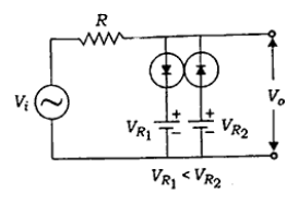
Draw the waveform of output $V_{0}$ and explain the operation of circuit with AC source $V_i$, Resistor R, Parallel diode clippers with bias voltages $V_{R1}$ and $V_{R2}$.

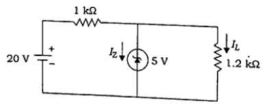
In the given circuit, calculate the load current $I_{L}$ and Zener diode current $I_{Z}$ with 20V source, 1k$\Omega$ resistor, 5V Zener diode, 1.2k$\Omega$ Load $R_L$.

Q.3 Solve both questions:
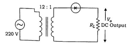
Calculate the maximum DC voltage and DC current available from a half-wave rectifier. What is the PIV of the diode used in the rectifier?

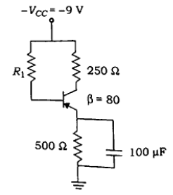
Calculate the value of $R_{1}$ in the biasing circuit, so that the Q-point is fixed at $I_{C}=8~mA$ and $V_{CE}=3~V$ with $-V_{CC} = -9V$, 250$\Omega$ collector resistor, 500$\Omega$ emitter resistor, $\beta=80$.

Q.4 Solve both questions:
Minimize the given Boolean function F using K map in SOP and implement using NAND gate: $F(A,B,C,D)=AB\overline{C}D+\overline{A}BCD+\overline{A}\overline{B}\overline{C} $ + $ \overline{A}\overline{B}\overline{D}+A\overline{C}+A\overline{B}C+\overline{B}C$
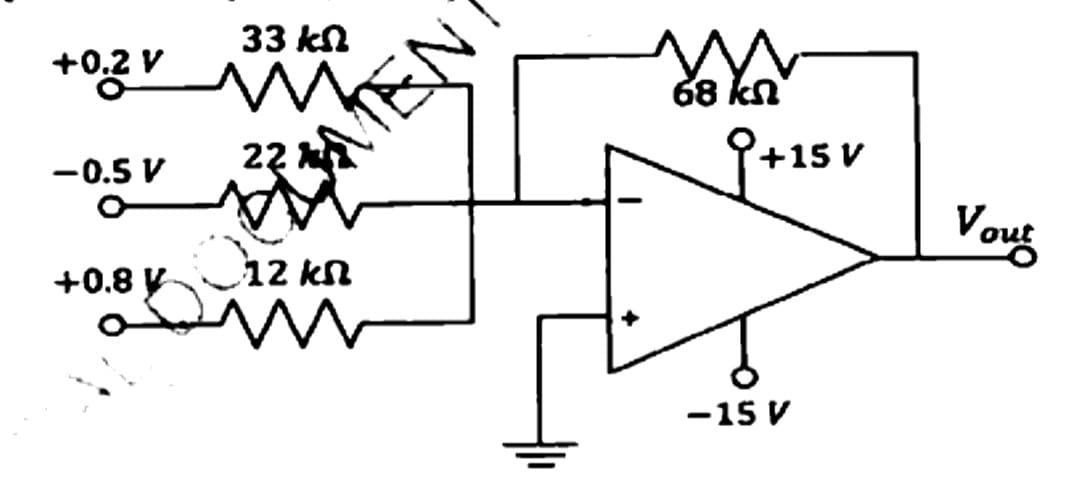
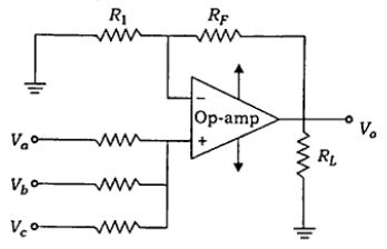
The circuit given is the basic application of op-amp to perform the addition operation. Explain the operation of circuit and derive the expression of output voltage.
Q.5 Solve both questions:
Design the voltage follower using op-amp and explain the operation.
Draw the circuit diagram of voltage-shunt feedback amplifier and derive the expression of closed-loop voltage gain.
Q.6 Solve both questions:
Draw the block diagram of cellular network and briefly explain its operation.
Draw the functional block diagram of AM transmitter and receiver.
Q.7 Solve both questions:
Design Schmitt trigger using IC 555 timer and explain its operation with the help of functional diagram.
If $R_{1}=R_{2}=R_{3}=450~k\Omega$ and $C_{1}=C_{2}=C_{3}=60pF$, determine the frequency of oscillation in phase-shift oscillator. Draw the basic circuit of an R-C phase-shift oscillator and explain its operation.
Q.8 Solve both questions:
A new clocked X-Y flip-flop is defined with inputs X and Y in addition to the clock input. The
flip-flop functions are as follows:
If XY=00 the flip-flop changes state with each clock
pulse.
If XY=01 the flip-flop state Q becomes 1 with the next clock pulse.
If XY=10,
the
flip-flop state Q becomes 0 with the next clock pulse.
If XY=11, no change of state occurs
with the clock pulse.
Write the truth table and excitation table of X-Y flip-flop.
Implement
the X-Y flip-flop using a J-K flip-flop.
What is the race around condition in J-K flip-flop? What are the methods to resolve the race around condition in J-K flip-flop? Explain each method with the help of example.
Q.9 Solve both questions:
What are the problems with normal encoder? How can these problems be solved by the priority decoder? Design 2 to 4 lines priority encoder.
Draw the block diagram of micro-controller and briefly explain each block.
Instructions:
- The marks are indicated in the right-hand margin.
- There are NINE questions in this paper.
- Attempt FIVE questions in all.
- Question No. 1 is compulsory.
Q.1 Answer the following questions (any seven) :
Why is negative feedback desired in amplifier application?
Draw the voltage transfer curve of op-amp.
State the Barkhausen's criteria for electronic system to oscillate with feedback.
How is amplifier different from the oscillator?
Why is the reception in the case of amplitude modulation usually noisy?
What is cell splitting and how does it increase the capacity of cellular network?
Justify that BJT is current controlled while FET is voltage-controlled device.
Name the breakdown mechanism in the lightly doped P-N junction diode under reverse biased condition.
Why is Gray code also called as reflected code? Convert to Gray code.
For the logical circuit shown in the figure below, derive the simplified Boolean expression for output Y.
Q.2 Solve both questions :
Draw the waveform of output and explain the operation of circuit in the figure given below.
Calculate the value of in the biasing circuit in the figure given below, so that the Q-point is fixed at and .
Q.3 Solve both questions :
Calculate the maximum DC voltage and DC current available from a half-wave rectifier shown in the figure given below. What is the PIV of the diode used in the rectifier?
In the figure given below, calculate the load current and Zener diode current $ I_Z $.
Q.4 Solve both questions :
Minimize the given Boolean function F using K map in SOP and implement using NAND gate: $ F(A,B,C,D) = AB\overline{C}D + \overline{A}BCD \overline{A}\overline{B}\overline{C} + \overline{A}\overline{B}\overline{D} + A\overline{C} + A\overline{B}C + \overline{B}C $
The circuit given below is the basic application of op-amp to perform the addition operation: Explain the operation of circuit and derive the expression of output voltage.
Q.5 Solve both questions :
Design the voltage follower using op-amp and explain the operation.
Draw the circuit diagram of voltage-shunt feedback amplifier and derive the expression of closed-loop voltage gain.
Q.6 Solve both questions :
Draw the block diagram of cellular network and briefly explain its operation.
Draw the functional block diagram of AM transmitter and receiver.
Q.7 Solve both questions :
Design Schmitt trigger using IC 555 timer and explain its operation with the help of functional diagram.
Draw the basic circuit of an R-C phase-shift oscillator and explain its operation. If $ R_1=R_2=R_3=450 \text{ k}\Omega C_1=C_2=C_3=60 \text{ pF} $, determine the frequency of oscillation in phase-shift oscillator.
Q.8 Solve both questions :
A new clocked X-Y flip-flop is defined with inputs X and Y in addition to the clock input. The flip-flop functions are as follows: If the flip-flop changes state with each clock pulse. If the flip-flop state Q becomes 1 with the next clock pulse. If , the flip-flop state Q becomes 0 with the next clock pulse. If , no change of state occurs with the clock pulse. Write the truth table and excitation table of X-Y flip-flop. Implement the X-Y flip-flop using a J-K flip-flop.
What is the race around condition in J-K flip-flop? What are the methods to resolve the race around condition in J-K flip-flop? Explain each method with the help of example.
Q.9 Solve both questions :
What are the problems with normal encoder? How can these problems be solved by the priority decoder? Design 2 to 4 lines priority encoder.
Draw the block diagram of micro-controller and briefly explain each block.
Instructions:
- The marks are indicated in the right-hand margin.
- There are NINE questions in this paper.
- Attempt FIVE questions in all.
- Question No. 1 is compulsory.
Q.1 Answer the following questions (any seven) :
Why is negative feedback desired in amplifier application?
Draw the voltage transfer curve of op-amp.
State the Barkhausen's criteria for electronic system to oscillate with feedback.
How is amplifier different from the oscillator?
Why is the reception in the case of amplitude modulation usually noisy?
What is cell splitting and how does it increase the capacity of cellular network?
Justify that BJT is current controlled while FET is voltage-controlled device.
Name the breakdown mechanism in the lightly doped P-N junction diode under reverse biased condition.
Why is Gray code also called as reflected code? Convert $ (396)_{10} $ to Gray code.
For the logical circuit shown in the figure below, derive the simplified Boolean expression for output Y.

Q.2 Solve both questions :
Draw the waveform of output $ V_0 $ and explain the operation of circuit in the figure given below.

Calculate the value of $ R_1 $ in the biasing circuit in the figure given below, so that the Q-point is fixed at $ I_C = 8 \text{ mA} $ and $ V_{CE} = 3 \text{ V} $.

Q.3 Solve both questions :
Calculate the maximum DC voltage and DC current available from a half-wave rectifier shown in the figure given below. What is the PIV of the diode used in the rectifier?

In the figure given below, calculate the load current $ I_L $ and Zener diode current $ I_Z $.

Q.4 Solve both questions :
Minimize the given Boolean function F using K map in SOP and implement using NAND gate: $ F(A,B,C,D) = AB\overline{C}D + \overline{A}BCD $ + $ \overline{A}\overline{B}\overline{C} + \overline{A}\overline{B}\overline{D} + A\overline{C} + A\overline{B}C + \overline{B}C $
The circuit given below is the basic application of op-amp to perform the addition operation: Explain the operation of circuit and derive the expression of output voltage.

Q.5 Solve both questions :
Design the voltage follower using op-amp and explain the operation.
Draw the circuit diagram of voltage-shunt feedback amplifier and derive the expression of closed-loop voltage gain.
Q.6 Solve both questions :
Draw the block diagram of cellular network and briefly explain its operation.
Draw the functional block diagram of AM transmitter and receiver.
Q.7 Solve both questions :
Design Schmitt trigger using IC 555 timer and explain its operation with the help of functional diagram.
Draw the basic circuit of an R-C phase-shift oscillator and explain its operation. If $ R_1=R_2=R_3=450 \text{ k}\Omega $ and $ C_1=C_2=C_3=60 \text{ pF} $, determine the frequency of oscillation in phase-shift oscillator.
Q.8 Solve both questions :
A new clocked X-Y flip-flop is defined with inputs X and Y in addition to the clock input. The
flip-flop functions are as follows:
If $ XY=00 $ the flip-flop changes state with each clock pulse.
If $ XY=01 $ the flip-flop state Q becomes 1 with the next clock pulse.
If $ XY=10 $, the flip-flop state Q becomes 0 with the next clock pulse.
If $ XY=11 $, no change of state occurs with the clock pulse.
Write the truth table and excitation table of X-Y flip-flop. Implement the X-Y flip-flop using a
J-K flip-flop.
What is the race around condition in J-K flip-flop? What are the methods to resolve the race around condition in J-K flip-flop? Explain each method with the help of example.
Q.9 Solve both questions :
What are the problems with normal encoder? How can these problems be solved by the priority decoder? Design 2 to 4 lines priority encoder.
Draw the block diagram of micro-controller and briefly explain each block.
Instructions:
- The marks are indicated in the right-hand margin.
- There are NINE questions in this paper.
- Attempt FIVE questions in all.
- Question No. 1 is compulsory.
Q.1 Answer the following questions (any seven) :
Why is negative feedback desired in amplifier application?
Draw the voltage transfer curve of op-amp.
State the Barkhausen's criteria for electronic system to oscillate with feedback.
How is amplifier different from the oscillator?
Why is the reception in the case of amplitude modulation usually noisy?
What is cell splitting and how does it increase the capacity of cellular network?
Justify that BJT is current controlled while FET is voltage-controlled device.
Name the breakdown mechanism in the lightly doped P-N junction diode under reverse biased condition.
Why is Gray code also called as reflected code? Convert to Gray code.
For the logical circuit shown in the figure below, derive the simplified Boolean expression for output Y.
Q.2 Solve both questions :
Draw the waveform of output and explain the operation of circuit in the figure given below.
Calculate the value of in the biasing circuit in the figure given below, so that the Q-point is fixed at and .
Q.3 Solve both questions :
Calculate the maximum DC voltage and DC current available from a half-wave rectifier shown in the figure given below. What is the PIV of the diode used in the rectifier?
In the figure given below, calculate the load current and Zener diode current $ I_Z $.
Q.4 Solve both questions :
Minimize the given Boolean function F using K map in SOP and implement using NAND gate: $ F(A,B,C,D) = AB\overline{C}D + \overline{A}BCD \overline{A}\overline{B}\overline{C} + \overline{A}\overline{B}\overline{D} + A\overline{C} + A\overline{B}C + \overline{B}C $
The circuit given below is the basic application of op-amp to perform the addition operation: Explain the operation of circuit and derive the expression of output voltage.
Q.5 Solve both questions :
Design the voltage follower using op-amp and explain the operation.
Draw the circuit diagram of voltage-shunt feedback amplifier and derive the expression of closed-loop voltage gain.
Q.6 Solve both questions :
Draw the block diagram of cellular network and briefly explain its operation.
Draw the functional block diagram of AM transmitter and receiver.
Q.7 Solve both questions :
Design Schmitt trigger using IC 555 timer and explain its operation with the help of functional diagram.
Draw the basic circuit of an R-C phase-shift oscillator and explain its operation. If $ R_1=R_2=R_3=450 \text{ k}\Omega C_1=C_2=C_3=60 \text{ pF} $, determine the frequency of oscillation in phase-shift oscillator.
Q.8 Solve both questions :
A new clocked X-Y flip-flop is defined with inputs X and Y in addition to the clock input. The
flip-flop functions are as follows:
If the flip-flop changes state with each clock pulse.
If the flip-flop state Q becomes 1 with the next clock pulse.
If , the flip-flop state Q becomes 0 with the next clock pulse.
If , no change of state occurs with the clock pulse.
Write the truth table and excitation table of X-Y flip-flop. Implement the X-Y flip-flop using a
J-K flip-flop.
What is the race around condition in J-K flip-flop? What are the methods to resolve the race around condition in J-K flip-flop? Explain each method with the help of example.
Q.9 Solve both questions :
What are the problems with normal encoder? How can these problems be solved by the priority decoder? Design 2 to 4 lines priority encoder.
Draw the block diagram of micro-controller and briefly explain each block.
Instructions:
- The marks are indicated in the right-hand margin.
- There are NINE questions in this paper.
- Attempt FIVE questions in all.
- Question No. 1 is compulsory.
Q.1 Answer the following questions (any seven):
Why is negative feedback desired in amplifier application?
Draw the voltage transfer curve of op-amp.
State the Barkhausen's criteria for electronic system to oscillate with feedback.
How is amplifier different from the oscillator?
Why is the reception in the case of amplitude modulation usually noisy?
What is cell splitting and how does it increase the capacity of cellular network?
Justify that BJT is current controlled while FET is voltage-controlled device.
Name the breakdown mechanism in the lightly doped P-N junction diode under reverse biased condition.
Why is Gray code also called as reflected code? Convert $(396)_{10}$ to Gray code.
For the logical circuit shown in the figure, derive the simplified Boolean expression for output Y.

Q.2 Solve both questions:
Draw the waveform of output $V_{0}$ and explain the operation of circuit with AC source $V_i$, Resistor R, Parallel diode clippers with bias voltages $V_{R1}$ and $V_{R2}$.
In the given circuit, calculate the load current $I_{L}$ and Zener diode current $I_{Z}$ with 20V source, 1k$\Omega$ resistor, 5V Zener diode, 1.2k$\Omega$ Load $R_L$.
Q.3 Solve both questions:
Calculate the maximum DC voltage and DC current available from a half-wave rectifier. What is the PIV of the diode used in the rectifier?
Calculate the value of $R_{1}$ in the biasing circuit, so that the Q-point is fixed at $I_{C}=8~mA$ and $V_{CE}=3~V$ with $-V_{CC} = -9V$, 250$\Omega$ collector resistor, 500$\Omega$ emitter resistor, $\beta=80$.
Q.4 Solve both questions:
Minimize the given Boolean function F using K map in SOP and implement using NAND gate: $F(A,B,C,D)=AB\overline{C}D+\overline{A}BCD+\overline{A}\overline{B}\overline{C} $ + $ \overline{A}\overline{B}\overline{D}+A\overline{C}+A\overline{B}C+\overline{B}C$
The circuit given is the basic application of op-amp to perform the addition operation. Explain the operation of circuit and derive the expression of output voltage.

Q.5 Solve both questions:
Design the voltage follower using op-amp and explain the operation.
Draw the circuit diagram of voltage-shunt feedback amplifier and derive the expression of closed-loop voltage gain.
Q.6 Solve both questions:
Draw the block diagram of cellular network and briefly explain its operation.
Draw the functional block diagram of AM transmitter and receiver.
Q.7 Solve both questions:
Design Schmitt trigger using IC 555 timer and explain its operation with the help of functional diagram.
If $R_{1}=R_{2}=R_{3}=450~k\Omega$ and $C_{1}=C_{2}=C_{3}=60pF$, determine the frequency of oscillation in phase-shift oscillator. Draw the basic circuit of an R-C phase-shift oscillator and explain its operation.
Q.8 Solve both questions:
A new clocked X-Y flip-flop is defined with inputs X and Y in addition to the clock input. The
flip-flop functions are as follows:
If XY=00 the flip-flop changes state with each clock
pulse.
If XY=01 the flip-flop state Q becomes 1 with the next clock pulse.
If XY=10,
the
flip-flop state Q becomes 0 with the next clock pulse.
If XY=11, no change of state occurs
with the clock pulse.
Write the truth table and excitation table of X-Y flip-flop.
Implement
the X-Y flip-flop using a J-K flip-flop.
What is the race around condition in J-K flip-flop? What are the methods to resolve the race around condition in J-K flip-flop? Explain each method with the help of example.
Q.9 Solve both questions:
What are the problems with normal encoder? How can these problems be solved by the priority decoder? Design 2 to 4 lines priority encoder.
Draw the block diagram of micro-controller and briefly explain each block.
Instructions:
- The marks are indicated in the right-hand margin.
- There are NINE questions in this paper.
- Attempt FIVE questions in all.
- Question No. 1 is compulsory.
Q.1 Answer the following questions (any seven) :
Why is negative feedback desired in amplifier application?
Draw the voltage transfer curve of op-amp.
State the Barkhausen's criteria for electronic system to oscillate with feedback.
How is amplifier different from the oscillator?
Why is the reception in the case of amplitude modulation usually noisy?
What is cell splitting and how does it increase the capacity of cellular network?
Justify that BJT is current controlled while FET is voltage-controlled device.
Name the breakdown mechanism in the lightly doped P-N junction diode under reverse biased condition.
Why is Gray code also called as reflected code? Convert $ (396)_{10} $ to Gray code.
For the logical circuit shown in the figure below, derive the simplified Boolean expression for output Y.
Q.2 Solve both questions :
Draw the waveform of output $ V_0 $ and explain the operation of circuit in the figure given below.
Calculate the value of $ R_1 $ in the biasing circuit in the figure given below, so that the Q-point is fixed at $ I_C = 8 \text{ mA} $ and $ V_{CE} = 3 \text{ V} $.
Q.3 Solve both questions :
Calculate the maximum DC voltage and DC current available from a half-wave rectifier shown in the figure given below. What is the PIV of the diode used in the rectifier?
In the figure given below, calculate the load current $ I_L $ and Zener diode current $ I_Z $.
Q.4 Solve both questions :
Minimize the given Boolean function F using K map in SOP and implement using NAND gate: $ F(A,B,C,D) = AB\overline{C}D + \overline{A}BCD $ + $ \overline{A}\overline{B}\overline{C} + \overline{A}\overline{B}\overline{D} + A\overline{C} + A\overline{B}C + \overline{B}C $
The circuit given below is the basic application of op-amp to perform the addition operation: Explain the operation of circuit and derive the expression of output voltage.
Q.5 Solve both questions :
Design the voltage follower using op-amp and explain the operation.
Draw the circuit diagram of voltage-shunt feedback amplifier and derive the expression of closed-loop voltage gain.
Q.6 Solve both questions :
Draw the block diagram of cellular network and briefly explain its operation.
Draw the functional block diagram of AM transmitter and receiver.
Q.7 Solve both questions :
Design Schmitt trigger using IC 555 timer and explain its operation with the help of functional diagram.
Draw the basic circuit of an R-C phase-shift oscillator and explain its operation. If $ R_1=R_2=R_3=450 \text{ k}\Omega $ and $ C_1=C_2=C_3=60 \text{ pF} $, determine the frequency of oscillation in phase-shift oscillator.
Q.8 Solve both questions :
A new clocked X-Y flip-flop is defined with inputs X and Y in addition to the clock input. The
flip-flop functions are as follows:
If $ XY=00 $ the flip-flop changes state with each clock pulse.
If $ XY=01 $ the flip-flop state Q becomes 1 with the next clock pulse.
If $ XY=10 $, the flip-flop state Q becomes 0 with the next clock pulse.
If $ XY=11 $, no change of state occurs with the clock pulse.
Write the truth table and excitation table of X-Y flip-flop. Implement the X-Y flip-flop using a
J-K flip-flop.
What is the race around condition in J-K flip-flop? What are the methods to resolve the race around condition in J-K flip-flop? Explain each method with the help of example.
Q.9 Solve both questions :
What are the problems with normal encoder? How can these problems be solved by the priority decoder? Design 2 to 4 lines priority encoder.
Draw the block diagram of micro-controller and briefly explain each block.