Instructions:
- The marks are indicated in the right-hand margin.
- There are NINE questions in this paper.
- Attempt FIVE questions in all.
- Question No. 1 is compulsory.
Q.1 Choose the correct option / answer the following (Any seven question
only):
When a pure semiconductor is heated, its resistance will
The random motion of holes and free electrons due to thermal agitation is called
A zener diode is used as
The ripple factor of a half-wave rectifier is
The number of depletion layers in a transistor is
In a transistor, $ I_{C}=100~mA $ and $ I_{E}=100.2~mA $. The value of $ \beta $ is
A non inverting closed loop op-amp circuit generally has a gain factor
If ground is applied to the (+) terminal of an inverting op-amp, the (-) terminal will
The binary code of (21.125) is
Which of the following gate is a two-level logic gate
Q.2 Solve both questions :
Explain the working of p-n junction diode and draw its V-I Characteristics.
Draw a neat circuit diagram of bridge rectifier and explain its operation with output waveforms. Derive the average value of current and voltage.
Q.3 Solve both questions :
Explain working principle of Depletion type MOSFET (n-channel). Draw & Explain its characteristics.
Explain the working principle and characteristics of a full-wave rectifier. Derive the expressions for output voltage and ripple factor for a full-wave rectifier.
Q.4 Solve both questions :
Draw the block diagram of Op-Amp and list all the ideal characteristics of op-amp.
Explain the working of op-amp as an Integrator and derive its output equation.
Q.5 Solve both questions :
Draw the circuit of NPN transistor in common base configuration and discuss its working. Draw input-output characteristic.
Explain the output and transfer characteristics of a JFET. How does the gate-source voltage $ (V_{GS}) $ affect the drain current $ (I_D) $?
Q.6 Solve both questions :
Convert the following:
(i) $ (53.625)_{10} $ to $ (?)_{2} $
(ii) Find the base x if $ (211)_{x}=(152)_{8} $
(iii) Subtract using 1's complement: $ (10111) - (110011) $
(iv) Find the 1's and 2's compliment of $ (010100)_2 $
Discuss the working of basic logic gates: NAND, NOR, XOR. Derive the truth tables and Boolean expressions for each gate.
Q.7 Solve both questions :
Explain the concept of load line analysis in a BJT. Derive the expressions for the load line and operating point. Explain their significance in amplifier design.
Explain the difference between intrinsic and extrinsic semiconductors. How does the addition of impurities affect the electrical properties of semiconductors?
Q.8 Solve both questions :
Discuss the working principle of clipping circuits. What are the different types of clipping circuits?
Explain the concepts of static and dynamic resistance in a diode. Derive expressions for both and discuss their significance in diode operation.
Q.9 Write short notes on any two of the following:
Solar cell
Basic logic gates, their symbols and truth tables
Clipping and Clamping circuits
Transistor biasing techniques
Instructions:
- The marks are indicated in the right-hand margin.
- There are NINE questions in this paper.
- Attempt FIVE questions in all.
- Question No. 1 is compulsory.
Section A
Choose the correct answer of the following (Any seven question only) :
The average value of the full-wave rectified sine wave with period and a peak value of is
The most commonly used transistor configuration for use as a switching device is
The Gunn diode is made of
If for a silicon N-P-N transistor, the base - to - emitter voltage is 0.7V and the collector - to - base voltage is 0.2V, then the transistor is operating in the
What current does represent in pn junction diode?
For normal operation of a transistor,
Transistor is in saturation when
If a differential amplifier has a gain of 20,000 and CMRR = 80 dB, its common mode gain is
An operational amplifier possesses
If the input ($V_{in}$) to the circuit is a sine wave, the output will be : [Diagram: A diode circuit taking input $V_{in}$]
Section B
Answer the following:
With a neat circuit diagram and waveform, explain the working of bridge rectifier.
Explain Zener diode as voltage regular with no load.
Answer the following:
Explain the operation of enhancement MOSFET.
Draw the DC load line for transistor and identify Q point.
Answer the following:
With a neat circuit diagram, explain the working of wein bridge oscillator using op-Amp.
Explain common base input characteristic of BJT.
Answer the following:
An amplifier with open loop voltage gain is available. It is required to have amplifier whose gain varies by not more than . Find (i) Reverse transmission factor of the feedback network, (ii) Gain with feedback.
Define, four basic ways of connection the feedback signal. Such as voltage-series feedback, voltage-shunt feedback, current-series feedback, current-shunt feedback.
Answer the following:
Explain the differences between BJT & FET.
Calculate the output voltage of the circuit shown in figure. The input voltages are and . [Diagram: Summing/difference op-amp circuit with to 1k, to 3.3k, non-inverting terminal to 1.5k, and feedback resistor 2.2k.]
Draw and explain pin configuration of 741 OP-Amp.
What is an SCR? Explain its working with switching characteristics.
Write short notes on any two of the following :
Differential amplifier
Explain positive half wave rectifier with input and output waveforms
Define OP-Amp parameter Gain, CMRR, Slew rate, Input Resistance.
Explain inverting amplifier.
Instructions:
- The marks are indicated in the right-hand margin.
- There are NINE questions in this paper.
- Attempt FIVE questions in all.
- Question No. 1 is compulsory.
Section A
Answer the following questions (any seven only):
Define Doping.
What are the two types of extrinsic semiconductors?
Write any two differences between Zener breakdown and Avalanche breakdown.
What materials are used to construct an LED?
What is transistor? Give its circuit symbol.
Give the relation between and .
Why base made thin in BJT?
What are the applications of JFET?
What are the differences between JFET and MOSFET?
Write Shockley's equation.
Section B
Answer the following:
With a neat diagrams explain the working of a PN junction diode in forward bias and reverse bias and plot the V-I characteristics.
Explain the switching characteristic of PN junction diode.
Answer the following:
Draw and Explain V-I characteristics of Zener diode.
With neat diagram explain the construction and working of LED.
Answer the following:
With a neat sketch explain the operation of CLC (ie section) and LC filter.
Describe the working principle of full wave rectifier with centre tapped transformer and derive the expressions for the ripple factor and efficiency.
Answer the following:
Explain the working of NPN and PNP transistor.
Draw and explain the input and output characteristics of a transistor in CC configuration.
Answer the following:
Explain Zener Diode as a Voltage Regulator.
Explain the working of positive clamping circuit.
Explain the construction, working and operating characteristics of N-Channel JFET's with relevant diagrams.
Describe the kind of operation that takes place in the enhancement mode MOSFET. How does this differ from depletion mode type?
Write Short notes on any two of the following:
Characteristics of an Ideal Operational Amplifier
Difference between Inverting and non inverting amplifier
Effects of negative feedback in amplifiers
Various topologies of feedback amplifier
Instructions:
- The marks are indicated in the right-hand margin.
- There are NINE questions in this paper.
- Attempt FIVE questions in all.
- Question No. 1 is compulsory.
Section A
Choose the correct answer of the following (Any seven question only) :
What is the ripple factor of a half-wave rectifier?
Which of the following is true in construction of a transistor?
For what kind of amplifications can the active region of the common-emitter configuration be used?
The leakage current in a pn junction is of the order of
A zener diode is always .......... connected.
The effective channel length of MOSFET in saturation decreases with increase in
A BJT with has base to collector leakage current of . If the transistor is connected in CE configuration, the collector current for is.
The threshold voltage of an n-channel enhancement type MOSFET is 0.5 V. When the device is biased at a gate voltage of 3 V, pinch-off would occur at a drain voltage of :
In an op-amp, the input impedance is .......... and the output impedance is .......... .
A MOSFET can be operated with .......... .
Section B
Answer the following:
Draw the diagram & Explain the working of full-wave rectifier with filter.
A half-wave rectifier is used to supply 50V d.c. to a resistive load of . The diode has a resistance of . Calculate the a.c. voltage required.
Answer the following:
Explain the working of current series feedback amplifier with the help of block diagram.
Explain about the distortions present in amplifier. List advantages of negative feedback.
Answer the following:
Draw V-I characteristics curves of JFET and mark various regions Explain how FET is voltage controlled device.
Draw the block diagram and explain the operation of sweep frequency generator.
Answer the following:
Draw the cross-sectional view of an n-p-n transistor and explain its operation in active region of operation. What are the different current components of the transistor? How can one use a transistor as amplifier?
Define and . Derive the relationship between and . If the base current in a transistor is , when the emitter current is , what are the values of and ? Also, calculate the collector current.
Answer the following:
Draw and explain the input and output characteristics of CB configuration. Where can we use the CB configuration in a transistor circuit? Explain with proper justification.
Explain the construction and working principle of a photo diode.
Answer the following:
Explain the characteristics of an Ideal Op-Amp.
Explain Op-amp as Differentiator and Integrator. Also draw the output Waveforms?
Answer the following:
With a neat diagram explain the working of a PN junction diode in forward bias and reverse bias.
Consider a pn junction in equilibrium at room temperature (T=300 K) for which the doping concentrations are and and the cross-sectional area . Calculate , and . Use .
Explain the following (attempt any two) :
Voltage divider bias network
Clipper and Clamper
Drift and Diffusion current
Instructions:
- The marks are indicated in the right-hand margin.
- There are NINE questions in this paper.
- Attempt FIVE questions in all.
- Question No. 1 is compulsory.
Section A
Answer the following questions briefly (any seven) :
Compute the collector current if base current is and current gain is 70.
Define ripple as referred to in a rectifier circuit.
A Zener diode has how many p-n junctions?
Write the formula for total power dissipated by a transistor in terms of voltage and current associated to transistor circuit.
What is the value of for a C-E configuration, when a silicon transistor is forward biased?
In a base resistor method, if the value of changes by 50, then by what factor collector current will change?
In voltage divider bias, . , , and . What is the emitter voltage?
When drain voltage equals the pinch-off-voltage, then what will happen to drain current if drain voltage increases?
At which point in JFET biasing, the JFET is not longer able to control the current?
Why is an SCR made of silicon and not germanium?
Section B
Answer the following:
Explain Hall effect phenomenon and list out its applications. Quantitatively discuss the use of Hall effect to determine mobility.
Define static and dynamic resistances of diode. What are their uses?
Answer the following:
In the circuit given below, the Zener voltage ($V_Z$) = 6 V, knee current ($I_Z$) = 6 mA and maximum power dissipated in Zener diode ($P_{max}$) = 0.4 W. Compute maximum and minimum values of such that for the satisfactory operation of this circuit : [Diagram: Zener regulator with source 15V, series resistor , Zener diode in series with a 5V source, and output voltage across load resistor .]
Draw the circuit diagram of full-wave bridge rectifier and give its input and output waveforms. Also derive the expression for the DC current.
Answer the following:
Explain the working of full-wave bridge rectifier with the help of its circuit diagram, input and output waveforms. List the advantages and disadvantages of this rectifier.
Define stabilization factors S, S' and S''. Derive the expression of S for fixed bias transistor circuit.
Answer the following:
A transistor amplifier connected in CE mode has and . Compute the values of and .
Explain the working of RC low-pass filter and draw its frequency response. Compute the cut-off frequency if RC circuit consisting of a resistor of in series with a capacitor of 60 nF.
Answer the following:
Compute the stability factor S for emitter feedback bias circuit. How the stability of Q-point is better in emitter feedback bias compare to fixed bias circuit?
Why is an FET known as a unipolar device? How do you compare this device with BJT?
Answer the following:
Data sheet of an EMOSFET specifies the following parameters : at and , the threshold voltage for EMOSFET is equal to 3 V. Determine the drain current at .
Explain thermal runaway. Show graphically that thermal runaway cannot take place if the quiescent point is located at .
Answer the following:
An inverting op-amp has and . Find the voltage gain of the amplifier. Also find the amplifier input resistance, input current and the output voltage, if the Input voltage is 0.2 V. Assume op-amp to be ideal.
Discuss a current-series feedback amplifier and compute the expression for transconductance using low-frequency approximate h-model of amplifier with an unbypassed emitter resistance.
Answer the following:
Draw the V-I characteristic of silicon-controlled rectifier (SCR) and explain different parameters of the curve. Explain any two SCR triggering or turn-on methods.
Explain the characteristics of an ideal op-amp. Mention two applications of op-amp. Draw the integrator circuit using op-amp.
Instructions:
- The marks are indicated in the right-hand margin.
- There are NINE questions in this paper.
- Attempt FIVE questions in all.
- Question No. 1 is compulsory.
Q.1 Fill in the blanks/Answer any seven of the following:
In CB configuration, output characteristics may be shown by plot of _______.
The _______ carriers enter the channel region through the _______ terminal and leave the channel through the _______ terminal in JFET.
Mention the advantages of Wien bridge oscillator.
What is reverse leakage current in CE configuration?
How is amplifier different from the oscillator?
Name the breakdown mechanism in the lightly doped P-N junction diode under reverse biased condition.
Draw the V-I characteristics of photodiode.
What is transconductance with reference to JFET?
What is the effect of removing bypass capacitor across the emitter resistor in case of CE amplifier?
What is meant by phase reversal?
Q.2 Solve both questions:
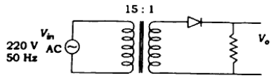
Find the DC voltage, ripple factor and efficiency for the half-wave rectifier given in the circuit. What should be PIV of the diode used? If bridge rectifier is used for same power supply, what will be the value of DC voltage and PIV of diode?
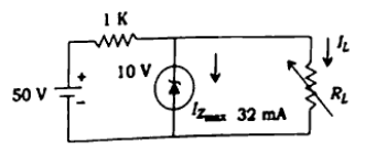
Calculate the range of $I_{L}$ and $R_{L}$ so that $V_{RL}$ being maintained at 10 V and also calculate the value of maximum voltage rating in the circuit with 50V source, 1K series resistor, 10V Zener with $I_{Zmax}$ 32 mA, Variable $R_L$.

Q.3 Solve both questions:
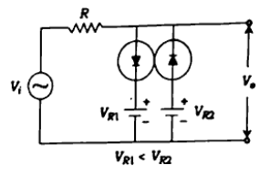
Draw the waveform of output $v_{0}$ and explain the operation of circuit with AC source $v_i$, Resistor R, Parallel clippers with diodes and batteries $V_{R1}$ and $V_{R2}$ where $V_{R1} < V_{R2}$.
Discuss the application of SCR as a power control with the help of circuit diagram.
Q.4 Solve both questions:
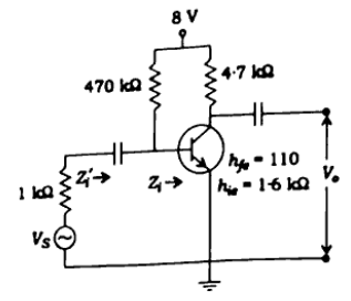
For the network given, determine the following parameters using the approximate equivalent model: Voltage gain $A_{v}$, current gain $A_{i}$, input impedance $Z_{i}'$ and $Z_{i}$.
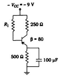
Calculate the value of $R_{1}$ in the biasing circuit so that the Q-point is fixed at $I_{C}=8~mA$ and $V_{CE}=3V$ with $V_{CC} = -9V$, 250$\Omega$ collector resistor, 500$\Omega$ emitter resistor, $\beta=80$.

Q.5 Solve both questions:
Given a depletion-type MOSFET. In the positive $v_{GS}$ region, does the drain current increase at a significantly higher rate than for negative value? Does the $I_{D}$ curve become more and more vertical with increasing positive values of $V_{GS}$?
Draw V-I characteristic curves of JFET and mark various regions. Explain how FET is voltage-controlled device.
Q.6 Solve both questions:
Explain the working of single-stage common emitter amplifier with the help of circuit diagram. Draw and explain the DC load-line analysis of this amplifier.
A single-stage amplifier has voltage gain of 10 and bandwidth of 1 MHz. Three such stages are cascaded and negative feedback of 10% is applied to the cascade stage. Find out the overall voltage gain and bandwidth of cascade stage with feedback.
Q.7 Solve both questions:
Explain the operation of Colpitts oscillator with the help of circuit diagram.
Draw the block diagram and explain the operation of sweep frequency generator.
Q.8 Solve both questions:
Discuss with the help of circuit diagram, the purpose of providing negative feedback and positive feedback.
Draw the circuit diagram of voltage-shunt feedback amplifier and derive the expression of closed-loop voltage gain using op-amp.
Q.9 Solve both questions:
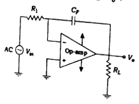
Explain the operation performed by the circuit with AC $v_{in}$, Resistor $R_1$, Capacitor $C_F$ in feedback, Load $R_L$ and derive the expression of output voltage $v_{0}$.

Op-amp can be used to add the DC voltage (addition operation). Draw the circuit and explain the operation of adder using op-amp in non-inverting mode.
Instructions:
- The marks are indicated in the right-hand margin.
- There are NINE questions in this paper.
- Attempt FIVE questions in all.
- Question No. 1 is compulsory.
Q.1 Fill in the blanks/Answer any seven of the following:
In CB configuration, output characteristics may be shown by plot of ______
The carriers enter the channel region through the ______ terminal and leave the channel through the ______ terminal in JFET.
Mention the advantages of Wien bridge oscillator.
What is reverse leakage current in CE configuration?
How is amplifier different from the oscillator?
Name the breakdown mechanism in the lightly doped P-N junction diode under reverse biased condition.
Draw the V-I characteristics of photodiode.
What is transconductance with reference to JFET?
What is the effect of removing bypass capacitor across the emitter resistor in case of CE amplifier?
What is meant by phase reversal?
Q.2 Solve both questions :
Find the DC voltage, ripple factor and efficiency for the half-wave rectifier given in the circuit below: What should be PIV of the diode used? If bridge rectifier is used for same power supply, what will be the value of DC voltage and PIV of diode?
Calculate the range of and so that being maintained at 10 V and also calculate the value of maximum voltage rating in the circuit given below :
Q.3 Solve both questions :
Draw the waveform of output and explain the operation of circuit given below: (Refer to question paper for circuit diagram)
Discuss the application of SCR as a power control with the help of circuit diagram.
Q.4 Solve both questions :
For the network given below, determine the following parameters using the approximate equivalent model. Voltage gain , current gain , input impedance and $ Z_i $:
Calculate the value of in the biasing circuit in the figure given below so that the Q-point is fixed at and :
Q.5 Solve both questions :
Given a deletion-type MOSFET. In the positive region, does the drain current increase at a significantly higher rate than for negative value? Does the curve become more and more vertical with increasing positive values of ?
Draw V-I characteristic curves of JFET and mark various regions. Explain how FET is voltage-controlled device.
Q.6 Solve both questions :
Explain the working of single-stage common emitter amplifier with the help of circuit diagram. Draw and explain the DC load-line analysis of this amplifier.
A single-stage amplifier has voltage gain of 10 and bandwidth of 1 MHz. Three such stages are cascaded and negative feedback of 10% is applied to the cascade stage. Find out the overall voltage gain and bandwidth of cascade stage with feedback.
Q.7 Solve both questions :
Explain the operation of Colpitts oscillator with the help of circuit diagram.
Draw the block diagram and explain the operation of sweep frequency generator.
Q.8 Solve both questions :
Discuss with the help of circuit diagram, the purpose of providing negative feedback and positive feedback.
Draw the circuit diagram of voltage-shunt feedback amplifier and derive the expression of closed-loop voltage gain using op-amp.
Q.9 Solve both questions :
Explain the operation performed by the circuit given below and derive the expression of output voltage :
Op-amp can be used to add the DC voltage (addition operation). Draw the circuit and explain the operation of adder using op-amp in non-inverting mode.
Instructions:
- The marks are indicated in the right-hand margin.
- There are NINE questions in this paper.
- Attempt FIVE questions in all.
- Question No. 1 is compulsory.
Q.1 Fill in the blanks/Answer any seven of the following:
In CB configuration, output characteristics may be shown by plot of ______
The carriers enter the channel region through the ______ terminal and leave the channel through the ______ terminal in JFET.
Mention the advantages of Wien bridge oscillator.
What is reverse leakage current in CE configuration?
How is amplifier different from the oscillator?
Name the breakdown mechanism in the lightly doped P-N junction diode under reverse biased condition.
Draw the V-I characteristics of photodiode.
What is transconductance with reference to JFET?
What is the effect of removing bypass capacitor across the emitter resistor in case of CE amplifier?
What is meant by phase reversal?
Q.2 Solve both questions :
Find the DC voltage, ripple factor and efficiency for the half-wave rectifier given in the circuit below: What should be PIV of the diode used? If bridge rectifier is used for same power supply, what will be the value of DC voltage and PIV of diode?

Calculate the range of $ I_L $ and $ R_L $ so that $ V_{RL} $ being maintained at 10 V and also calculate the value of maximum voltage rating in the circuit given below :

Q.3 Solve both questions :
Draw the waveform of output $ v_0 $ and explain the operation of circuit given below: (Refer to question paper for circuit diagram)

Discuss the application of SCR as a power control with the help of circuit diagram.
Q.4 Solve both questions :
For the network given below, determine the following parameters using the approximate equivalent model. Voltage gain $ A_v $, current gain $ A_i $, input impedance $ Z_i' $ and $ Z_i $:

Calculate the value of $ R_1 $ in the biasing circuit in the figure given below so that the Q-point is fixed at $ I_C = 8 \text{ mA} $ and $ V_{CE} = 3\text{V} $:

Q.5 Solve both questions :
Given a deletion-type MOSFET. In the positive $ v_{GS} $ region, does the drain current increase at a significantly higher rate than for negative value? Does the $ I_D $ curve become more and more vertical with increasing positive values of $ v_{GS} $?
Draw V-I characteristic curves of JFET and mark various regions. Explain how FET is voltage-controlled device.
Q.6 Solve both questions :
Explain the working of single-stage common emitter amplifier with the help of circuit diagram. Draw and explain the DC load-line analysis of this amplifier.
A single-stage amplifier has voltage gain of 10 and bandwidth of 1 MHz. Three such stages are cascaded and negative feedback of 10% is applied to the cascade stage. Find out the overall voltage gain and bandwidth of cascade stage with feedback.
Q.7 Solve both questions :
Explain the operation of Colpitts oscillator with the help of circuit diagram.
Draw the block diagram and explain the operation of sweep frequency generator.
Q.8 Solve both questions :
Discuss with the help of circuit diagram, the purpose of providing negative feedback and positive feedback.
Draw the circuit diagram of voltage-shunt feedback amplifier and derive the expression of closed-loop voltage gain using op-amp.
Q.9 Solve both questions :
Explain the operation performed by the circuit given below and derive the expression of output voltage $ v_0 $:

Op-amp can be used to add the DC voltage (addition operation). Draw the circuit and explain the operation of adder using op-amp in non-inverting mode.
Instructions:
- The marks are indicated in the right-hand margin.
- There are NINE questions in this paper.
- Attempt FIVE questions in all.
- Question No. 1 is compulsory.
Q.1 Fill in the blanks/Answer any seven of the following:
In CB configuration, output characteristics may be shown by plot of ______
The carriers enter the channel region through the ______ terminal and leave the channel through the ______ terminal in JFET.
Mention the advantages of Wien bridge oscillator.
What is reverse leakage current in CE configuration?
How is amplifier different from the oscillator?
Name the breakdown mechanism in the lightly doped P-N junction diode under reverse biased condition.
Draw the V-I characteristics of photodiode.
What is transconductance with reference to JFET?
What is the effect of removing bypass capacitor across the emitter resistor in case of CE amplifier?
What is meant by phase reversal?
Q.2 Solve both questions :
Find the DC voltage, ripple factor and efficiency for the half-wave rectifier given in the circuit below: What should be PIV of the diode used? If bridge rectifier is used for same power supply, what will be the value of DC voltage and PIV of diode?
Calculate the range of and so that being maintained at 10 V and also calculate the value of maximum voltage rating in the circuit given below :
Q.3 Solve both questions :
Draw the waveform of output and explain the operation of circuit given below: (Refer to question paper for circuit diagram)
Discuss the application of SCR as a power control with the help of circuit diagram.
Q.4 Solve both questions :
For the network given below, determine the following parameters using the approximate equivalent model. Voltage gain , current gain , input impedance and $ Z_i $:
Calculate the value of in the biasing circuit in the figure given below so that the Q-point is fixed at and :
Q.5 Solve both questions :
Given a deletion-type MOSFET. In the positive region, does the drain current increase at a significantly higher rate than for negative value? Does the curve become more and more vertical with increasing positive values of ?
Draw V-I characteristic curves of JFET and mark various regions. Explain how FET is voltage-controlled device.
Q.6 Solve both questions :
Explain the working of single-stage common emitter amplifier with the help of circuit diagram. Draw and explain the DC load-line analysis of this amplifier.
A single-stage amplifier has voltage gain of 10 and bandwidth of 1 MHz. Three such stages are cascaded and negative feedback of 10% is applied to the cascade stage. Find out the overall voltage gain and bandwidth of cascade stage with feedback.
Q.7 Solve both questions :
Explain the operation of Colpitts oscillator with the help of circuit diagram.
Draw the block diagram and explain the operation of sweep frequency generator.
Q.8 Solve both questions :
Discuss with the help of circuit diagram, the purpose of providing negative feedback and positive feedback.
Draw the circuit diagram of voltage-shunt feedback amplifier and derive the expression of closed-loop voltage gain using op-amp.
Q.9 Solve both questions :
Explain the operation performed by the circuit given below and derive the expression of output voltage :
Op-amp can be used to add the DC voltage (addition operation). Draw the circuit and explain the operation of adder using op-amp in non-inverting mode.
Instructions:
- The marks are indicated in the right-hand margin.
- There are NINE questions in this paper.
- Attempt FIVE questions in all.
- Question No. 1 is compulsory.
Q.1 Fill in the blanks/Answer any seven of the following:
In CB configuration, output characteristics may be shown by plot of ______
The carriers enter the channel region through the ______ terminal and leave the channel through the ______ terminal in JFET.
Mention the advantages of Wien bridge oscillator.
What is reverse leakage current in CE configuration?
How is amplifier different from the oscillator?
Name the breakdown mechanism in the lightly doped P-N junction diode under reverse biased condition.
Draw the V-I characteristics of photodiode.
What is transconductance with reference to JFET?
What is the effect of removing bypass capacitor across the emitter resistor in case of CE amplifier?
What is meant by phase reversal?
Q.2 Solve both questions :
Find the DC voltage, ripple factor and efficiency for the half-wave rectifier given in the circuit below: What should be PIV of the diode used? If bridge rectifier is used for same power supply, what will be the value of DC voltage and PIV of diode?
Calculate the range of and so that being maintained at 10 V and also calculate the value of maximum voltage rating in the circuit given below :
Q.3 Solve both questions :
Draw the waveform of output and explain the operation of circuit given below: (Refer to question paper for circuit diagram)
Discuss the application of SCR as a power control with the help of circuit diagram.
Q.4 Solve both questions :
For the network given below, determine the following parameters using the approximate equivalent model. Voltage gain , current gain , input impedance and $ Z_i $:
Calculate the value of in the biasing circuit in the figure given below so that the Q-point is fixed at and :
Q.5 Solve both questions :
Given a deletion-type MOSFET. In the positive region, does the drain current increase at a significantly higher rate than for negative value? Does the curve become more and more vertical with increasing positive values of ?
Draw V-I characteristic curves of JFET and mark various regions. Explain how FET is voltage-controlled device.
Q.6 Solve both questions :
Explain the working of single-stage common emitter amplifier with the help of circuit diagram. Draw and explain the DC load-line analysis of this amplifier.
A single-stage amplifier has voltage gain of 10 and bandwidth of 1 MHz. Three such stages are cascaded and negative feedback of 10% is applied to the cascade stage. Find out the overall voltage gain and bandwidth of cascade stage with feedback.
Q.7 Solve both questions :
Explain the operation of Colpitts oscillator with the help of circuit diagram.
Draw the block diagram and explain the operation of sweep frequency generator.
Q.8 Solve both questions :
Discuss with the help of circuit diagram, the purpose of providing negative feedback and positive feedback.
Draw the circuit diagram of voltage-shunt feedback amplifier and derive the expression of closed-loop voltage gain using op-amp.
Q.9 Solve both questions :
Explain the operation performed by the circuit given below and derive the expression of output voltage :
Op-amp can be used to add the DC voltage (addition operation). Draw the circuit and explain the operation of adder using op-amp in non-inverting mode.
Instructions:
- The marks are indicated in the right-hand margin.
- There are NINE questions in this paper.
- Attempt FIVE questions in all.
- Question No. 1 is compulsory.
Q.1 Fill in the blanks/Answer any seven of the following:
In CB configuration, output characteristics may be shown by plot of _______.
The _______ carriers enter the channel region through the _______ terminal and leave the channel through the _______ terminal in JFET.
Mention the advantages of Wien bridge oscillator.
What is reverse leakage current in CE configuration?
How is amplifier different from the oscillator?
Name the breakdown mechanism in the lightly doped P-N junction diode under reverse biased condition.
Draw the V-I characteristics of photodiode.
What is transconductance with reference to JFET?
What is the effect of removing bypass capacitor across the emitter resistor in case of CE amplifier?
What is meant by phase reversal?
Q.2 Solve both questions:
Find the DC voltage, ripple factor and efficiency for the half-wave rectifier given in the circuit. What should be PIV of the diode used? If bridge rectifier is used for same power supply, what will be the value of DC voltage and PIV of diode?

Calculate the range of $I_{L}$ and $R_{L}$ so that $V_{RL}$ being maintained at 10 V and also calculate the value of maximum voltage rating in the circuit with 50V source, 1K series resistor, 10V Zener with $I_{Zmax}$ 32 mA, Variable $R_L$.
Q.3 Solve both questions:
Draw the waveform of output $v_{0}$ and explain the operation of circuit with AC source $v_i$, Resistor R, Parallel clippers with diodes and batteries $V_{R1}$ and $V_{R2}$ where $V_{R1} < V_{R2}$.

Discuss the application of SCR as a power control with the help of circuit diagram.
Q.4 Solve both questions:
For the network given, determine the following parameters using the approximate equivalent model: Voltage gain $A_{v}$, current gain $A_{i}$, input impedance $Z_{i}'$ and $Z_{i}$.

Calculate the value of $R_{1}$ in the biasing circuit so that the Q-point is fixed at $I_{C}=8~mA$ and $V_{CE}=3V$ with $V_{CC} = -9V$, 250$\Omega$ collector resistor, 500$\Omega$ emitter resistor, $\beta=80$.
Q.5 Solve both questions:
Given a depletion-type MOSFET. In the positive $v_{GS}$ region, does the drain current increase at a significantly higher rate than for negative value? Does the $I_{D}$ curve become more and more vertical with increasing positive values of $V_{GS}$?
Draw V-I characteristic curves of JFET and mark various regions. Explain how FET is voltage-controlled device.
Q.6 Solve both questions:
Explain the working of single-stage common emitter amplifier with the help of circuit diagram. Draw and explain the DC load-line analysis of this amplifier.
A single-stage amplifier has voltage gain of 10 and bandwidth of 1 MHz. Three such stages are cascaded and negative feedback of 10% is applied to the cascade stage. Find out the overall voltage gain and bandwidth of cascade stage with feedback.
Q.7 Solve both questions:
Explain the operation of Colpitts oscillator with the help of circuit diagram.
Draw the block diagram and explain the operation of sweep frequency generator.
Q.8 Solve both questions:
Discuss with the help of circuit diagram, the purpose of providing negative feedback and positive feedback.
Draw the circuit diagram of voltage-shunt feedback amplifier and derive the expression of closed-loop voltage gain using op-amp.
Q.9 Solve both questions:
Explain the operation performed by the circuit with AC $v_{in}$, Resistor $R_1$, Capacitor $C_F$ in feedback, Load $R_L$ and derive the expression of output voltage $v_{0}$.
Op-amp can be used to add the DC voltage (addition operation). Draw the circuit and explain the operation of adder using op-amp in non-inverting mode.
Instructions:
- The marks are indicated in the right-hand margin.
- There are NINE questions in this paper.
- Attempt FIVE questions in all.
- Question No. 1 is compulsory.
Q.1 Fill in the blanks/Answer any seven of the following:
In CB configuration, output characteristics may be shown by plot of ______
The carriers enter the channel region through the ______ terminal and leave the channel through the ______ terminal in JFET.
Mention the advantages of Wien bridge oscillator.
What is reverse leakage current in CE configuration?
How is amplifier different from the oscillator?
Name the breakdown mechanism in the lightly doped P-N junction diode under reverse biased condition.
Draw the V-I characteristics of photodiode.
What is transconductance with reference to JFET?
What is the effect of removing bypass capacitor across the emitter resistor in case of CE amplifier?
What is meant by phase reversal?
Q.2 Solve both questions :
Find the DC voltage, ripple factor and efficiency for the half-wave rectifier given in the circuit below: What should be PIV of the diode used? If bridge rectifier is used for same power supply, what will be the value of DC voltage and PIV of diode?
Calculate the range of $ I_L $ and $ R_L $ so that $ V_{RL} $ being maintained at 10 V and also calculate the value of maximum voltage rating in the circuit given below :
Q.3 Solve both questions :
Draw the waveform of output $ v_0 $ and explain the operation of circuit given below: (Refer to question paper for circuit diagram)
Discuss the application of SCR as a power control with the help of circuit diagram.
Q.4 Solve both questions :
For the network given below, determine the following parameters using the approximate equivalent model. Voltage gain $ A_v $, current gain $ A_i $, input impedance $ Z_i' $ and $ Z_i $:
Calculate the value of $ R_1 $ in the biasing circuit in the figure given below so that the Q-point is fixed at $ I_C = 8 \text{ mA} $ and $ V_{CE} = 3\text{V} $:
Q.5 Solve both questions :
Given a deletion-type MOSFET. In the positive $ v_{GS} $ region, does the drain current increase at a significantly higher rate than for negative value? Does the $ I_D $ curve become more and more vertical with increasing positive values of $ v_{GS} $?
Draw V-I characteristic curves of JFET and mark various regions. Explain how FET is voltage-controlled device.
Q.6 Solve both questions :
Explain the working of single-stage common emitter amplifier with the help of circuit diagram. Draw and explain the DC load-line analysis of this amplifier.
A single-stage amplifier has voltage gain of 10 and bandwidth of 1 MHz. Three such stages are cascaded and negative feedback of 10% is applied to the cascade stage. Find out the overall voltage gain and bandwidth of cascade stage with feedback.
Q.7 Solve both questions :
Explain the operation of Colpitts oscillator with the help of circuit diagram.
Draw the block diagram and explain the operation of sweep frequency generator.
Q.8 Solve both questions :
Discuss with the help of circuit diagram, the purpose of providing negative feedback and positive feedback.
Draw the circuit diagram of voltage-shunt feedback amplifier and derive the expression of closed-loop voltage gain using op-amp.
Q.9 Solve both questions :
Explain the operation performed by the circuit given below and derive the expression of output voltage $ v_0 $:
Op-amp can be used to add the DC voltage (addition operation). Draw the circuit and explain the operation of adder using op-amp in non-inverting mode.
Instructions:
- The marks are indicated in the right-hand margin.
- There are NINE questions in this paper.
- Attempt FIVE questions in all.
- Question No. 1 is compulsory.
Section A
Choose the correct option of the following (any seven) :
Which of the following expressions represents the correct formula for the density of electrons occupying the donor level?
What is the ripple factor of a half-wave rectifier?
Which of the following is true about the resistance of a Zener diode?
Which of the following is true in construction of a transistor?
Consider the following statements : A clamper circuit
- adds or subtracts a d.c. voltage to a waveform
- does not change the waveform
- amplifies the waveform Which are correct?
For what kind of amplifications can the active region of the common-emitter configuration be used?
How does the FET operate before the pinch-off region with small value of drain-to-source voltage in accordance to the control of drain-to-source resistance by the bias voltage?
A junction FET can operate in
Which of the following is not a property of an ideal operational amplifier?
Which among the following is the major responsible reason for the cause of 'slew rate'?
Section B
Answer the following:
Draw potential energy diagrams for a forward as well as a reverse-biased p-n junction and explain the flow of currents in both the cases.
The p-silicon has resistivity of . The other parameters for silicon are : Intrinsic carrier density, , Hole mobility, and Electron mobility, . Calculate the number of electrons for every 5000 million holes in the semiconductor.
Answer the following:
Determine and the required PIV rating of each diode for the configuration of the following figure : [Diagram: Bridge rectifier circuit with input sine wave (peak 100V), ideal diodes, and load resistor $R_L = 2.2 k\Omega$]. In addition, determine the maximum current through each diode.
The circuit shown below uses a 9V Zener diode. If the load resistance is equal to and the d.c. source equals 24V, find the maximum value of resistor R required to maintain a constant voltage of 9V across the load. [Diagram: Zener diode circuit with source , series resistor R, and parallel combination of Zener and load .]
Answer the following:
Draw the cross-sectional view of an n-p-n transistor and explain its operation in active region of operation. What are the different current components of the transistor? How can one use a transistor as amplifier?
Define and . Derive the relationship between and . If the base current in a transistor is , when the emitter current is , what are the values of and ? Also, calculate the collector current.
Answer the following:
Draw and explain the input and output characteristics of CB configuration. Where can we use the CB configuration in a transistor circuit? Explain with proper justification.
Design a collector to base bias circuit shown in the figure below for the specified conditions : . [Diagram: Collector-to-base bias circuit configuration.]
Answer the following:
Draw the structure of JFET and discuss its working. What is pinch-off voltage? How to get its value experimentally?
For the voltage-divider configuration of the figure shown below, determine : (i) and , (ii) and . [Diagram: JFET voltage divider bias circuit. . JFET parameters: .]
Answer the following:
Define an ideal operational amplifier. Draw the approximate block diagram of an OPAMP giving various stages of the amplifier.
Find the output voltage of the following OPAMP circuit : [Diagram: Inverting OPAMP circuit with non-inverting terminal grounded through 2k, inverting terminal connected to 12V via 2k, and feedback resistor 10k.]
Answer the following:
Draw the gain-frequency response of an RC coupled amplifier. Discuss fall in gain at very low and at very high frequencies.
Common emitter (CE) amplifier shown in the figure has voltage gain of 150 when . Stability is brought through negative feedback by adding resistor . Calculate the value of resistor using feedback concepts so that final voltage gain ($= A_{FB}$) is equal to 100. [Diagram: CE amplifier circuit with voltage divider bias and unbypassed emitter resistor .]
Answer the following:
Explain the construction and working principle of a photo diode (PD).
Explain the construction and working principle of an SCR. Write the applications utilizing SCR.
Instructions:
- The marks are indicated in the right-hand margin.
- There are NINE questions in this paper.
- Attempt FIVE questions in all.
- Question No. 1 is compulsory.
Q.1 Answer/Fill in the blanks/Write true or false (any seven):
Why is filter required to be added after rectifier circuit?
What is the application of voltage regulator?
DC value of pure AC waveform is ______.
Which of the transistor currents is always the largest?
What is the source of leakage current in a transistor?
What is the major difference between a bipolar and a unipolar device?
Give the advantage of negative feedback in amplifier.
BUT amplifier changes the frequency and shape of the signal.
CMMR for ideal operational amplifier is ______.
Slew rate for ideal operational amplifier is ______.
Q.2 Solve both questions :
Draw volt-ampere characteristics of a Zener diode. What is meant by the knee voltage in the curve?
Describe in detail the avalanche breakdown mechanism in a diode.
Q.3 Solve both questions :
Explain the principle of operation of LED with the help of diagram.
Derive the expression for $ I_C $ in terms of $ I_E $ and $ \alpha_{dc} $ for a common-base BUT configuration. For a given $ \alpha_{dc} $ of 0.998, determine $ I_C $, if $ I_E = 4 \, \text{mA} $.
Q.4 Solve both questions :
Define the stability factor. What does smaller stability factor indicate?
Derive the expression for stability factor for voltage divider bias (self-bias) circuit.
Q.5 Solve both questions :
Explain the construction and characteristics of FET.
Draw and explain h-parameter small signal model for BJT.
Q.6 Solve both questions :
Explain the working of common emitter amplifier with the help of circuit diagram.
What are the roles of coupling and bypass capacitors? Explain in detail.
Q.7 Solve both questions :
Describe the RC phase-shift oscillator with circuit diagram.
Explain the working of high-frequency LC oscillator with the help of circuit diagram.
Q.8 Solve both questions :
Explain the working of voltage series feedback amplifier with the help of block diagram.
Design an integrator using op-amp and explain its working.
Q.9 Solve both questions :
Write the circuit diagram of differential amplifier configurations and explain its working.
Explain about CMRR, slew rate and concept of virtual ground.
Instructions:
- The marks are indicated in the right-hand margin.
- There are NINE questions in this paper.
- Attempt FIVE questions in all.
- Question No. 1 is compulsory.
Q.1 Answer/Fill in the blanks/Write true or false (any seven):
Why is filter required to be added after rectifier circuit?
What is the application of voltage regulator?
DC value of pure AC waveform is ______
Which of the transistor currents is always the largest?
What is the source of leakage current in a transistor?
What is the major difference between a bipolar and a unipolar device?
Give the advantage of negative feedback in amplifier
BJT amplifier changes the frequency and shape of the signal. (True/False)
CMMR for ideal operational amplifier is ______
Slew rate for ideal operational amplifier is ______
Q.2 Solve both questions :
Draw volt-ampere characteristics of a Zener diode. What is meant by the knee voltage in the curve?
Describe in detail the avalanche breakdown mechanism in a diode.
Q.3 Solve both questions :
Explain the principle of operation of LED with the help of diagram.
Derive the expression for $ I_C $ in terms of $ I_E $ and $ \alpha_d $ for a common-base BJT configuration. For a given $ \alpha_d $ of 0.998, determine $ I_C $ if $ I_E = 4 \text{ mA} $.
Q.4 Solve both questions :
Define the stability factor. What does smaller stability factor indicate?
Derive the expression for stability factor for voltage divider bias (self-bias) circuit.
Q.5 Solve both questions :
Explain the construction and characteristics of FET.
Draw and explain h-parameter small signal model for BJT.
Q.6 Solve both questions :
Explain the working of common emitter amplifier with the help of circuit diagram.
What are the roles of coupling and bypass capacitors? Explain in detail.
Q.7 Solve both questions :
Describe the RC phase-shift oscillator with circuit diagram.
Explain the working of high-frequency LC oscillator with the help of circuit diagram.
Q.8 Solve both questions :
Explain the working of voltage series feedback amplifier with the help of block diagram.
Design an integrator using op-amp and explain its working.
Q.9 Solve both questions :
Write the circuit diagram of differential amplifier configurations and explain its working.
Explain about CMRR, slew rate and concept of virtual ground.
Instructions:
- The marks are indicated in the right-hand margin.
- There are NINE questions in this paper.
- Attempt FIVE questions in all.
- Question No. 1 is compulsory.
Section A
Answer the following questions briefly (any seven) :
If doping level in a crystal diode is increased, what will happen to the width of depletion layer?
How does Zener diode behave in the breakdown region?
At which voltage avalanche occurs in a diode?
If the maximum DC current rating of diodes in bridge rectifier is 2A, then what is the maximum DC load current?
A half-wave rectifier has an input voltage of 240 V r.m.s. If the step-down transformer has a turns ratio of 8 : 1, what is the peak load voltage? Ignore diode drop.
If , voltage-divider resistor is and is , what is the base bias voltage?
When does thermal runaway occur?
With the E-MOSFET, what is the value of drain current when gate input voltage is zero?
What is the bandwidth of an ideal operational amplifier?
If gate current is increased, then what will happen to anode-cathode voltage at which SCR closes?
Section B
Answer the following:
Differentiate between ideal and practical voltage sources. Give their graphical representations and convert voltage source with its series resistance of into its equivalent current source.
Derive continuity equation for carrier concentration in body of a semiconductor.
Answer the following:
Derive the expressions for (i) , (ii) , (iii) ripple factor and (iv) efficiency of rectification; in case of full-wave rectifier.
Draw a sketch to show various currents in an N-P-N transistor and derive the relationship between various components.
Answer the following:
A 4 : 1 transformer supplies a bridge rectifier that is driving a load of 400 ohms. If the transformer input is supply, calculate the d.c. output voltage, P-I-V and the output frequency. Assume the rectifier diodes to be ideal.
Draw diode I-V characteristics, discuss its temperature dependence and obtain the expression for diode dynamic resistance.
Answer the following:
Using a common collector N-P-N transistor configuration, derive the expressions for voltage gain and current gain.
Design the voltage divider bias circuit to operate from supply. The bias conditions are and .
Answer the following:
A collector to base circuit has and . Calculate and determine when a new transistor is replaced having .
Draw two-dimensional structure of n-channel MOSFET. Explain its working.
Answer the following:
An n-channel FET is utilized by amplifier shown in figure for which and . It is desired to bias the circuit at , using . Assume . Find (i) , (ii) and (iii) .
[Diagram: Self-bias JFET amplifier circuit with and bypass capacitor , coupling capacitor .]
Explain the working of BJT voltage divider bias circuit. Derive the expression for Q-point ($I_{CQ}, V_{CEQ}$) in terms of circuit parameters.
Answer the following:
Explain a voltage-series feedback amplifier with suitable example.
Using an op-amp, explain the circuits for a voltage gain amplifier (with least components) and current to voltage converter.
Answer the following:
Explain the working principle of unijunction transistor (UJT).
Describe the structure, symbol and operation of SCR with the help of suitable diagrams.
Instructions:
- The marks are indicated in the right-hand margin.
- There are NINE questions in this paper.
- Attempt FIVE questions in all.
- Question No. 1 is compulsory.
Section A
Answer any seven of the following questions :
Clipper and clamper are the applications of ________.
Give one application of Zener diode.
SCR is bistable device. (State True or False)
Which of the transistor currents is always the largest?
Sketch the common-base BJT transistor configuration (for n-p-n and p-n-p).
Why is coupling capacitor used in common-emitter amplifier?
Which BJT amplifier configuration has unity voltage gain?
Which BJT amplifier configuration has unity current gain?
Define conversion efficiency.
What is the highest efficiency of class A direct coupled amplifier?
Section B
Answer the following:
For the series connected diode configuration as given below in the figure, determine and :
[Diagram: Series circuit with 8V source, Si diode (marked +V_D-$), and resistor $R (marked $+V_R-$).]
Draw the diagram and explain the working of a full-wave rectifier with filter.
Answer the following:
Explain the working and applications of photodiode.
Explain the construction, operation and characteristics of SCR.
Answer the following:
Explain the working of common-collector amplifier as a voltage buffer.
Compute and explain common-emitter amplifier operating point and load line.
Answer the following:
Compare between depletion type MOSFET and enhancement type MOSFET.
Explain the working of common-base amplifier as a current buffer.
Answer the following:
Explain about the distortions present in amplifier. List the advantages of negative feedback.
Explain the working of current series feedback amplifier with the help of block diagram.
Answer the following:
Describe the working of Wien bridge oscillator circuit.
Design the R-C elements of a Wien bridge oscillator, when it operates at .
Answer the following:
Explain the working of a non-sinusoidal type of oscillator with the help of its circuit diagram.
Write and explain two applications of differential amplifier with the help of circuit diagrams.
Answer the following:
Write the properties of ideal operational amplifier.
Draw the pin configuration of 741 op-amp IC and explain its working.
Instructions:
- The marks are indicated in the right-hand margin.
- There are NINE questions in this paper.
- Attempt FIVE questions in all.
- Question No. 1 is compulsory.
Section A
Choose the correct answer of the following (any seven) :
When checking a diode, low resistance readings both ways indicate the diode is
Which of the following is the correct relationship between and ?
If a half-wave peak has an average voltage of , what is the average of two full-wave peaks?
The Q-point on a load line may be used to determine
For the BJT to operate in the active (linear) region, the base-emitter junction must be ________-biased and the base-collector junction must be ________-biased.
What is the level of drain current for gate-to-source voltages less than (more negative than) the pinch-off level?
How much times reverse saturation current will increase, if temperature increases ?
The total discharge time for the capacitor in a clamper having and is
How many op-amps are required to implement the equation ?
A non-inverting closed-loop op-amp circuit generally has a gain factor
Section B
Answer the following:
Differentiate between an ideal and a practical voltage source. Give their graphical representations and convert voltage source with its series resistance of into its equivalent current source.
Explain the working of a shunt capacitor filter and derive an approximate expression for ripple factor in half-wave rectifier with shunt capacitor filter.
Answer the following:
Compare the differences between JFET and MOSFET and also prove that the transconductance of a JFET is given by
Explain the UJT as a relaxation oscillator.
Answer the following:
Explain Zener and avalanche breakdown in semiconductors.
Define and of a transistor. Also derive the relationship between them.
Answer the following:
Sketch the output characteristics for N-channel JFET with gate-source shorted (i.e., $V_{GS} = 0$). How are ohmic, pinch off and breakdown regions created?
Explain the basic structure and working of a P-channel JFET.
Answer the following:
Compare the characteristics of CB, CE and CC configurations of a transistor. Draw the circuit of a common-collector transistor configuration and explain its operation. Also derive the relation between and current amplification factors.
A collector to base circuit has and . Calculate and determine when a new transistor is replaced having .
Answer the following:
An inverting op-amp has and . Find the voltage gain of the amplifier. Also find the amplifier input resistance, input current and the output voltage if the input voltage is . Assume op-amp to be ideal.
Explain the working of an op-amp as an integrator circuit.
Answer the following:
Explain a voltage-shunt feedback amplifier with suitable example.
In a transistor circuit, load resistance is and quiescent current is . Determine the operating point when the battery voltage . How will the Q-point change when the load resistance is changed from to ?
Answer the following:
Describe the structure, symbol and operation of SCR with the help of suitable diagrams.
In an N-type semiconductor, the Fermi level lies below the conduction band at . If the temperature is increased to , find the new position of the Fermi level.
Instructions:
- The marks are indicated in the right-hand margin.
- There are NINE questions in this paper.
- Attempt FIVE questions in all.
- Question No. 1 is compulsory.
Questions
Answer the following questions (any seven) :
State the most important SCR parameters for high-current devices.
State Fermi energy level ($E_F$) of an intrinsic semiconductor.
Define base width modulation.
Differentiate between drift current and diffusion current.
Define avalanche multiplication.
Define peak point current of a UJT.
State the definition of threshold voltage of a MOSFET.
Define CMRR of an op-amp.
State the applications of photodiode.
Why are PIV of bridge and centre-tapped full-wave rectifier not same?
Answer the following questions:
Accurately analyze the collector-to-base bias circuit is shown in figure 1 to determine the and , when (i) $\beta = 50$; (ii) . Assume . [Diagram Fig. 1: Voltage divider bias circuit with $V_{CC}=18\text{V}, R_{B1}=33\text{ k}\Omega, R_{B2}=12\text{ k}\Omega, R_C=1.2\text{ k}\Omega, R_E=1\text{ k}\Omega$]
With the help of a neat diagram, explain the input and output characteristics of common-collector (CC) configuration.
Answer the following questions:
With the help of band and bond models, explain both N-type and P-type extrinsic silicons.
A silicon p-n diode has a doping of and (for Si: $n_i = 1.5 \times 10^{10} \text{ cm}^{-3}, \epsilon_r = 11.9$). (i) Determine the depletion width in the n-region. (ii) Determine the built-in potential at . (iii) Calculate the depletion width when it biased to .
What do you mean by rectification? Explain the working of a half-wave rectifier circuit with resistive load. With sinusoidal input, derive the expressions for the following :
Average output voltage and current
RMS load current and voltage
Form factor and ripple factor
Efficiency
Answer the following questions:
Draw the circuit of a UJT relaxation oscillator with provision for frequency adjustment and spike waveform. Show all waveforms, and explain the circuit operation.
Draw the circuit diagram to show how an SCR can be triggered by the application of a pulse to gate terminal. Sketch the circuit waveforms and explain its operation.
Answer the following questions:
Explain the construction and characteristics of n-channel JFET.
The FET circuit is shown in figure 2 has and . Find its input impedance and output impedance and voltage gain. [Diagram Fig. 2: JFET amplifier with voltage divider bias ($R_1, R_2$), source resistor ($R_S$), and load ($R_L$)]
Answer the following questions:
Given and , determine (i) the common-emitter hybrid equivalent circuit; (ii) the common-base $r_e$-model.
Compare the advantages and disadvantages of biasing schemes in BJT.
Answer the following questions:
Draw the circuit diagram of a practical voltage series feedback amplifier and derive the expressions for input resistance, output resistance, voltage gain and current gain.
Explain the operation and characteristics of photodiode.
Answer the following questions:
Explain the summing and differential amplifiers using op-amp with derivation of output voltage.
Calculate the output voltages and in the circuit of the following figure 3 : [Diagram Fig. 3: Two-stage op-amp circuit. First stage is non-inverting ($R_f=20\text{k}\Omega, R_1=10\text{k}\Omega$), second stage is inverting ($R_{f2}=200\text{k}\Omega, R_{i2}=200\text{k}\Omega$)]
Instructions:
- There are Nine Questions in this Paper. All questions carry equal marks.
- Attempt Five questions in all.
- Question No. 1 is Compulsory.
- The marks are indicated in the right-hand margin.
Section A
Choose the correct alternatives for any seven of the following;
The junction capacitance of a linearly graded junction varies with the applied reverse voltage (V) as
Reverse saturation current in a silicon PN junction diode is doubled for every
A rectifier is used to
Polarity of dc output voltage of a half wave rectifier can be reversed by reversing
When a transistor operates in active region, it behaves as
If the Q-point of a transistor lies at ________, the negative part of input signal is clipped at output.
Trans-conductance of JFET is measured in
The threshold voltage of an enhancement pMOS transistor is
In a common-emitter amplifier, the unbiased emitter resistance provides
An ideal OP-AMP has
Section B
Answer the following:
What is a forward biased and reverse biased diode? How is the width of the space charge region and barrier height affected in forward biased and reversed diode?
What is the relation between current and voltage in a PN junction diode? Explain each term involved in that relation. The reverse saturation current of a silicon PN junction diode is at the temperature . Determine the forward bias voltage to be applied across the PN junction to obtain a current of about .
Answer the following:
Explain depletion layer capacitance and diffusion capacitance of a PN junction diode in detail. How do these capacitances vary with respect to applied bias voltage across a silicon PN-junction diode?
A silicon has a doping density of acceptors in the P-type region and a doping density of donors in the N-type region. Assume at room temperature of and the dielectric constant of silicon as . Determine the built in potential and the total space charge (depletion layer) width at .
Answer the following:
What is ripple factor? Why ripple factor is so important in power supply? Derive the expression of ripple factor of a full wave rectifier using centre-tap transformer.
A single phase full wave rectifier circuit consists of four diodes, a load resistance and it is fed from a ac power supply. The forward resistance of each diode is . Determine the dc output voltage, dc load current and efficiency.
Answer the following:
What is a bipolar junction transistor (BJT)? Why are these transistors called bipolar devices? What are the different configuration of BJT?
Derive the relation between and of a BJT.
The collector current of a transistor is and is is . Calculate the value of base current and emitter current.
Answer the following:
What are the different types of biasing? Derive the expression for stability factor of self bias circuit.
A voltage divider bias circuit of a BJT is shown in Fig.-1 below. Determine the emitter current and collector-to-emitter voltage. Calculate the collector potential Vc. Assume and .
[Diagram: Figure-1 - Voltage divider bias circuit of N-P-N transistor. $V_{CC}=18\text{V}, R_1=10\text{k}\Omega, R_2=9.5\text{k}\Omega, R_C=1.5\Omega, R_E=4.5\text{k}\Omega, V_{BE}=0.65, \beta=75$]
Answer the following:
Discuss the construction and working principle of a P-channel enhancement type MOSFET with diagrams and draw the device characteristics.
In an N-channel JFET, . Find the minimum value of for pinch off operation. Determine the value of drain current at .
Answer the following:
Draw the circuit diagram of an integrator using opamp and explain its operation. If a square wave voltage signal is applied at the input of an integrator then draw its out in same time scale of input signal.
Draw the circuit diagram of a non-inverting summing amplifier using opamp and determine the output voltage.
Write short notes on the following:
Photo diode
Unijunction Transistor
Instructions:
- There are Nine Questions in this Paper.
- Attempt Five questions in all.
- Question No. 1 is Compulsory.
- The marks are indicated in the right hand margin.
Questions
Answer the following questions:
Difference between BJT and MOSFET.
Define thermal run way.
Difference between depletion mode and enhancement mode MOSFET.
List the most important SCR parameters for low-current devices.
Emitter saturation voltage of UJT.
List the most important parameters of operational amplifier and their typical values.
Define the Pinch-off voltage JFET.
Define flat-band voltage.
State the applications of light emitting diode.
Why the BJT dimensions of Emitter, Base and Collector of are not same?
Answer the following questions:
Derive and explain an intrinsic carrier concentration ($n_i$) of a semiconductor.
Explain the operation and characteristics of light emitting diode.
Answer the following questions:
For the circuit shown in Figure 1, determine (i) d.c. output voltage (ii) rectification efficiency (iii) peak inverse voltage (iv) output frequency [Diagram: Center-tapped transformer with 10:1 ratio, 220V 50Hz input, bridge rectifier with four diodes, 250 ohm load resistor]
Explain the operation of silicon diode at equilibrium condition. Also derive the expression for the following : (i) Maximum electric field ($E_{max}$) (ii) Depletion width (W) (iii) Built-in potential ($V_{bi}$)
Answer the following questions:
Accurately analyze the collector-to-base bias circuit is shown in Figure 2 to determine the and when (i) and (ii) Assume . [Diagram: Collector-to-base bias circuit with $V_{CC}=18\text{V}, R_C=2.2\text{ k}\Omega, R_B=270\text{ k}\Omega$]
Sketch typical BJT common-emitter input and output characteristics. Explain the shapes of the characteristics.
Answer the following questions:
Draw the two biasing circuits for JFET and explain.
Derive the gain expression of an integrator and a differentiator using op-amp.
Answer the following questions:
Explain the basic operation and characteristics of n-channel depletion type MOSFET.
Sketch a phase control for an SCR. Draw the load waveform and explain the circuit operation.
Answer the following questions:
Draw Sketches to show the basic construction and equivalent circuit of a unijunction transistor (UJT). Briefly explain the device operation.
Design a clamper to perform the function shown in the Figure 3 shown below. [Diagram: Input pulse , output pulse to , Design block with input and output $V_{out}$]
Answer the following questions:
Briefly explain the small signal model of JFET.
An integrator using op-amp has following component values. and . A square wave applied to integrator. The amplifier uses supply and output saturates at if input alternates between then. (i) Determine the maximum change in output (ii) Determine the maximum slew rate.
Answer the following questions:
Define the gate power dissipation and explain its importance in SCR.
Explain the operation of centre tapped full wave rectifier. And calculate the rms load current and voltage for a sinusoidal input.
Instructions:
- The marks are indicated in the right-hand margin.
- There are NINE questions in this paper.
- Attempt FIVE questions in all.
- Question No. 1 is compulsory.
Questions
Choose the correct alternatives for any seven of the following :
The width of depletion layer of a P-N junction diode is (i) independent of applied voltage (ii) increased with applied reverse bias voltage (iii) increased with applied forward bias voltage (iv) increased with doping
A diffusion current flows through a P-N junction just after its formation due to (i) minority carriers (ii) majority carriers (iii) forward bias (iv) reverse bias
A half-wave rectifier is equivalent to a (i) clipping circuit (ii) clamper circuit (iii) clamper circuit with negative bias (iv) clamper circuit with positive bias
In an LC filter, the ripple factor (i) increases with load current (ii) increases with load resistance (iii) remains constant with load resistance (iv) decreases with load current
If collector-base junction is reverse biased and the emitter-base junction is forward biased, the transistor operates at (i) saturation region (ii) cut-off region (iii) active region (iv) All of the above
If the Q point of a transistor lies at ________, the positive part of input signal is clipped at output. (i) near saturation point (ii) near cut-off point (iii) middle of active region (iv) anywhere of the load line
The input impedance of a JFET is in the range of (i) above (ii) (iii) (iv)
The threshold voltage of an enhancement NMOS transistor is (i) less than zero volt (ii) equal to zero volt (iii) greater than zero volt (iv) None of the above
Which topology of feedback amplifier has very high input and output impedances? (i) Voltage series feedback (ii) Voltage shunt feedback (iii) Current series feedback (iv) Current shunt feedback
An ideal OP-AMP has (i) infinite input impedance (ii) zero output impedance (iii) infinite voltage gain (iv) All of the above
Answer the following questions:
Draw the energy-band diagram of an open-circuited P-N junction diode and derive the expression for contact difference potential across this open-circuited P-N junction diode.
At the room temperature of , the resistivities of the N-type region and P-type region of a germanium P-N junction are and respectively. Determine the contact potential and potential energy barrier at . Assume— , , .
Answer the following questions:
Explain how the process of avalanche breakdown occurs in P-N junction. How is it different from Zener breakdown?
Draw the circuit of a Zener diode shunt-regulated power supply. In this regulated power supply, required output voltage across load resistance is with load current . Input d.c. voltage varies from to . Determine the maximum and minimum Zener currents. [Consider $P_z(\text{max}) = 1000\text{ mW}$]
Answer the following questions:
What is transformer utilization factor? Derive the transformer utilization factor of a half-wave rectifier circuit. Discuss the difference between the half-wave and full-wave rectifier circuits.
The turn ratio of the transformer used in single-phase full-wave rectifier circuit is . The primary of transformer is connected to and a.c. supply. Determine the peak inverse voltage of each diode and output frequency. Assume all diodes are ideal.
Answer the following questions:
Draw the circuit diagram of an N-P-N junction transistor CE configuration and describe the static input and output characteristics. Also define active, saturation and cut-off regions and saturation resistance in CE configuration.
Derive the relation between and of a BJT.
A BJT has a base current , and . Calculate the collector current and emitter current.
Answer the following questions:
What do you mean by biasing? Why is it required? Define stability factors for biasing. What are the factors on which stability of biasing depends?
The voltage divider bias circuit of N-P-N transistor is shown in figure below. Calculate the values of and when collector current is and collector to emitter voltage is . Assume and . [Diagram: Voltage divider bias with $V_{CC}=6\text{V}, R_1, R_2=10\text{k}\Omega, R_C, R_E=350\text{ }\Omega$]
Answer the following questions:
Discuss the construction and working principle of an N-channel enhancement-type MOSFET with diagrams and draw the device characteristics.
In an N-channel JFET, and and . Determine the drain current and transconductance at .
Answer the following questions:
Draw the circuit diagram of a differentiator using OP-AMP and explain its operation. If a square-wave voltage signal is applied at the input of a differentiator, then draw its out in same timescale of input signal.
Draw the circuit diagram of an inverting summing amplifier using OP-AMP and determine the output voltage.
Write short notes on the following:
Light-emitting diode
Silicon-controlled rectifier
Instructions:
- (i) The marks are indicated in the right-hand margin.
- (ii) There are NINE questions in this paper.
- (iii) Attempt FIVE questions in all.
- (iv) Question No. 1 is compulsory.
Questions
Answer the following questions:
Why is silicon preferred over germanium in making of semiconductor devices?
What do you understand by transition capacitance of a diode?
Why we cannot measure the barrier potential of a diode using voltmeter?
Explain one disadvantage of bridge rectifier.
Capacitor filter is not suited for heavy loads. Why?
Answer the following questions:
Derive and explain an intrinsic carrier concentration ($n_i$) of a semiconductor.
Explain the operation and characteristics of light emitting diode.
Answer the following questions:
For the circuit shown in Figure 1, determine (i) d.c. output voltage (ii) rectification efficiency (iii) peak inverse voltage (iv) output frequency
Explain the operation of p-n silicon diode at equilibrium condition. Also derive the expression for the following: (i) Maximum electric field ($E_{max}$) (ii) Depletion width (W) (iii) Built-in potential ($V_{bi}$)
Answer the following questions:
Accurately analyze the collector-to-base bias circuit is shown in Figure 2 to determine the , and when (i) and (ii) . Assume V.
Sketch typical BJT common-emitter input and output characteristics. Explain the shapes of the characteristics.
Answer the following questions:
Draw the two biasing circuits for JFET and explain.
Derive the gain expression of an integrator and a differentiator using op-amp.
Answer the following questions:
Explain the basic operation and characteristics of n-channel depletion type MOSFET.
Sketch a phase control for an SCR. Draw the load waveform and explain the circuit operation.
Answer the following questions:
Draw Sketches to show the basic construction and equivalent circuit of a unijunction transistor (UJT). Briefly explain the device operation.
Design a clamper to perform the function shown in the Figure 3 shown below.
Answer the following questions:
Briefly explain the small signal model of JFET.
An integrator using op-amp has following component values: and . A square wave applied to integrator. The amplifier uses supply and output saturates at if input alternates between then: (i) Determine the maximum change in output (ii) Determine the maximum slew rate.
Answer the following questions:
Define the gate power dissipation and explain its importance in SCR.
Explain the operation of centre tapped full wave rectifier. And calculate the rms load current and voltage for a sinusoidal input.
Instructions:
- (i) The marks are indicated in the right-hand margin.
- (ii) There are NINE questions in this paper.
- (iii) Attempt FIVE questions in all.
- (iv) Question No. 1 is compulsory.
Questions
Choose the correct option of any seven of the following:
The mobility of an electron in a conductor is expressed in terms of
Current flow in a semiconductor depends on the phenomenon of
A certain amount of --- still flows when diode is under reverse biased condition.
Bridge rectifiers are preferred because
Transistor is
In a JFET, drain current is maximum when is
Input impedance of FET is
Which of the following will not decrease as a result of introduction of feedback?
In a common-emitter amplifier, the unbypassed emitter resistance provides
LEDs are fabricated from
Answer the following questions:
What is the concentration of holes in Si crystals having donor concentration of , when the intrinsic carrier concentration is ? Find the ratio of electrons to holes concentration.
Draw the V-I characteristic of Si and Ge diode on the same axis and explain.
Answer the following questions:
Explain the working of centre-tapped full-wave rectifier.
For the circuit of Fig. 1, determine the range of and that will result in being maintained at .
Answer the following questions:
Derive the relation between and of BJT.
Describe the working of NPN transistor and explain the input and output characteristics of common-emitter amplifier.
Answer the following questions:
Find and for the circuit shown in Fig. 2 for the BJT whose .
Draw and explain potential divider biasing circuit.
Answer the following questions:
List the advantages and disadvantages of FET over BJT.
Explain the working of JFET along with its transfer and output characteristics.
Answer the following questions:
What are the advantages of negative feedback in amplifiers? Explain them.
Draw the circuit diagram of voltage series feedback amplifier and derive the expression for input and output impedances.
Answer the following questions:
Name six important parameters of an operational amplifier. What are their ideal values and practical values?
Describe the working of OPAMP as an integrator and an inverter.
Write notes on the following:
SCR
LED
Instructions:
- The marks are indicated in the right-hand margin.
- There are NINE questions in this paper.
- Attempt FIVE questions in all.
- Question No. 1 is compulsory.
Questions
Choose the correct alternative of the following (any seven):
When a step-input is given to an op-amp integrator, the output will be (i) a ramp (ii) a sinusoidal wave (iii) a rectangular wave (iv) a triangular wave with d.c. bias
In a JFET, at pinch-off voltage applied on the gate (i) the drain current becomes almost zero (ii) the drain current begins to decrease (iii) the drain current is almost at saturation value (iv) the drain to source voltage is close to zero volt
The value of ripple factor of a half-wave rectifier without filter is approximately (i) 1.2 (ii) 0.2 (iii) 2.2 (iv) 2.0
In the voltage regulator shown in Fig. 1, if the current through the load decreases [Diagram: Zener voltage regulator with series resistor R1, Zener diode D, and load resistor RL] (i) the current through R1 will increase (ii) the current through R1 will decrease (iii) Zener diode current will increase (iv) Zener diode current will decrease
The lowest output impedance is obtained in case of BJT amplifiers for (i) CB configuration (ii) CE configuration (iii) CC configuration (iv) CE with configuration
What is the peak current through the resistor in the circuit shown in Fig. 2 assuming the diode to be ideal? [Diagram: AC source 12sin(omega t) in series with 1k ohm resistor, a diode, and a 4V battery opposing the source] (i) 4 mA (ii) 8 mA (iii) 12 mA (iv) 16 mA
Answer the following questions:
Explain how the process of avalanche breakdown occurs in a P-N junction diode. How is it different from Zener breakdown?
A silicon diode has a saturation current of at room temperature of . Determine its value at .
Answer the following questions:
For the circuit shown in Fig. 3 below: [Diagram: Zener regulator with . Input can vary from to $30\text{ V}$] Find— (i) the minimum and maximum currents in Zener diode; (ii) the minimum and maximum power dissipated in the diode.
Draw the voltage doubler circuit. Sketch input and output waveforms and explain the circuit operation.
Answer the following questions:
A simple full-wave bridge rectifier circuit has an input voltage of a.c. r.m.s. Assume the diodes to be ideal. Find the output d.c. current, d.c. voltage, r.m.s. values of output currents and voltages. Assume load resistance to be .
Explain and factors of transistors. Derive the expressions for them and state their meanings.
Answer the following questions:
In a self-biased CE amplifier, and . Compute the stability factor.
What is operating point? Explain its physical significance with proper example.
Answer the following questions:
State the advantages of FET over BJT.
Derive an expression for the gain of negative voltage feedback amplifier.
Answer the following questions:
What is clamping circuit? With neat diagram, explain different types of clampers.
Sketch for the network shown in Fig. 4 below. [Diagram: Input square wave applied to circuit with capacitor C, ideal diode D with bias, and resistor R]
Answer the following questions:
Compute the voltage gain and power gain of the amplifier circuit shown in Fig. 5 below: [Diagram: Op-amp amplifier with feedback resistor and input resistor]
Explain the turn-off mechanism of SCR.
Write short notes on the following:
UJT
Pi filter
Light-emitting diode (LED)
Integrator